
Method of fabricating novel seed layers for fabricating spin valve heads

a technology of giant magnetoresistive magnets and seed layers, which is applied in the field of fabrication of giant magnetoresistive (gmr) magnetic read heads, can solve the problems of insufficient performance and difficult accuracy of the sensing process, and achieve the effect of improving the output of the sensor and reducing the thickness of the seed layer

Active Publication Date: 2007-06-26
HEADWAY TECH INC
View PDF9 Cites 9 Cited by
  • Summary
  • Abstract
  • Description
  • Claims
  • Application Information

AI Technical Summary

Benefits of technology

[0013]A third object of this invention is to provide such a GMR sensor element of a single bottom spin valve type and of a dual symmetric spin valve type, each having synthetic antiferromagnetic (SyAF) pinned layers, ultra-thin ferromagnetic free layers, ultra-thin antiferromagnetic pinning layers, very high values of DR / R and relatively high sheet resistance.
[0014]A fourth object of this invention is to provide a method for forming an ultra-thin symmetric dual spin valve having a high signal-to-noise ratio resulting from a high bias current due to low sheet resistance and a very high value of DR / R and capable of reading recorded densities of up to 100 Gb / in2.
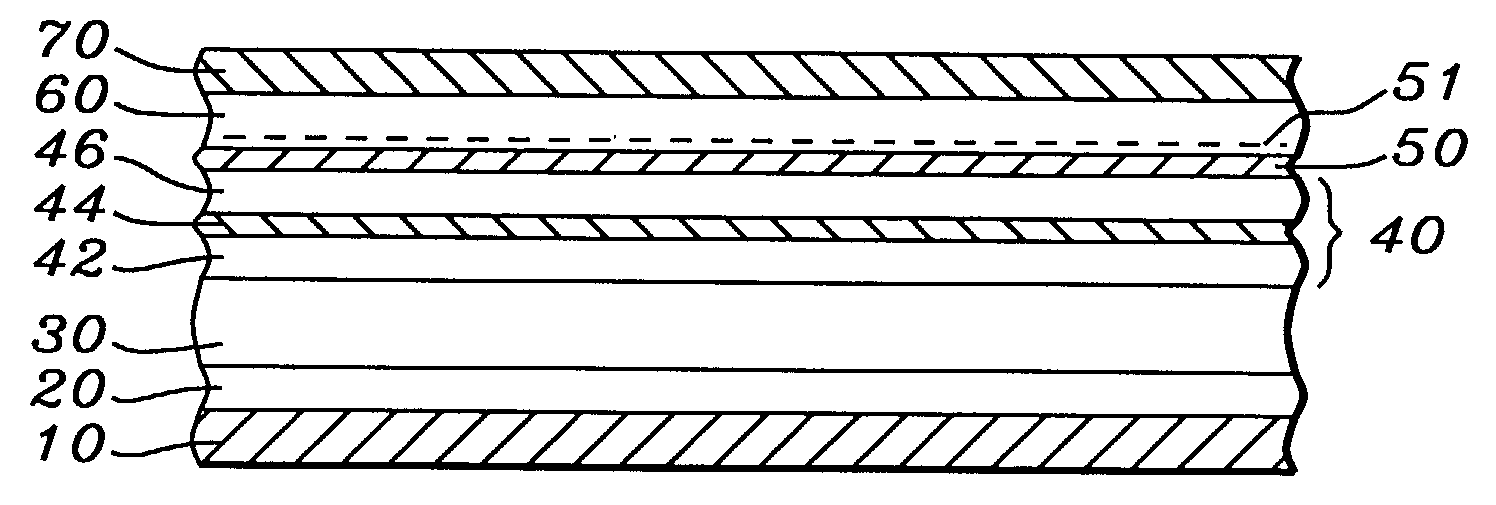
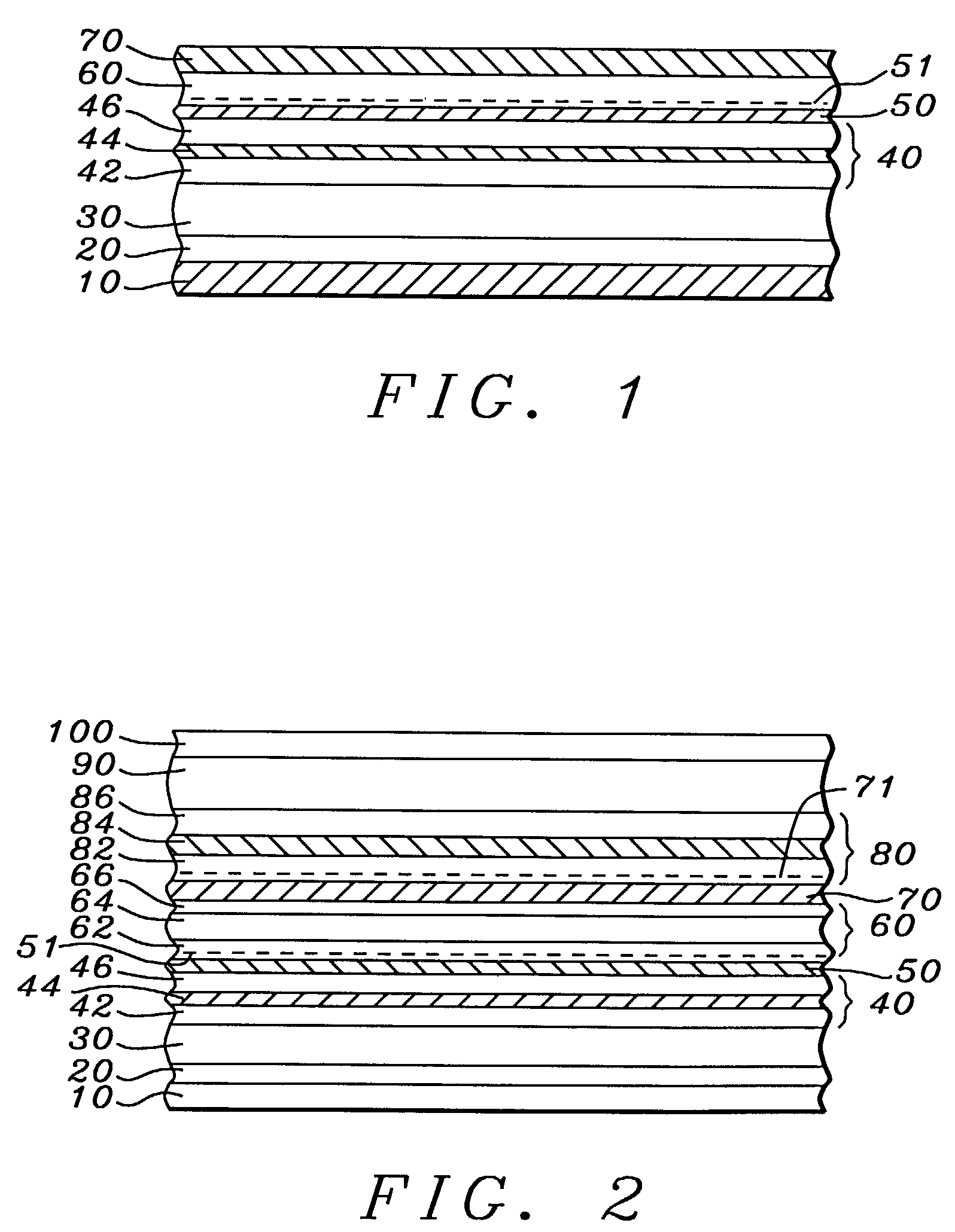
[0017]In a second embodiment there is provided a method of forming a symmetric dual spin valve sensor utilizing the same novel seed layer as in the first embodiment. To practice the method there is first provided a substrate. There is then formed upon the substrate the GMR effect-enhancing ultra-thin (approximately 30 angstroms) NiCr seed layer wherein the Ni is approximately 69 atomic percent and the Cr is approximately 31 atomic percent of the layer. There is then formed on this seed layer a correspondingly thin antiferromagnetic pinning layer of MnPt approximately 80 angstroms thick. On this pinning layer is then formed a first SyAF pinned layer, which is a tri-layer of CoFe / Ru / CoFe of the approximate dimensions 13 angstroms for the first CoFe layer, 7.5 angstroms for the Ru layer and 15 angstroms for the second CoFe layer. There is then formed on the SyAF a non-magnetic Cu spacer layer treated to form an oxygen surfactant layer (OSL). There is then formed on the OSL treated Cu layer an ultra-thin CoFe / NiFe / CoFe ferromagnetic free layer in which the first of the CoFe layers is approximately 5 angstroms thick, the NiFe layer is approximately 15 angstroms thick, and the second of the CoFe layers is approximately 3 angstroms thick, to complete a bottom spin-valve structure. There is then formed over this bottom spin-valve structure an OSL treated second Cu spacer layer, on which is then formed a second SyAF layer which is the mirror image of the first and a second MnPt layer approximately 70 angstroms thick to complete the symmetric dual spin valve. By reducing the thickness of the seed layer and the MnPt antiferromagnetic layer, a dual spin valve of only approximately 340 angstroms thickness can be formed. Moreover, the magnetostriction as measured by the coefficient lambda falls within the desirable range between 1.0E-06 and 2.0E-06, improving the output of the sensor. Such a thin sensor can easily fit between upper and lower magnetic shields in the read / write heads designed for ultra-high density recordings.

Problems solved by technology

This made the sensing process difficult to achieve with accuracy.
The present challenge to the spin valve form of sensor is to make it suitable for reading recorded magnetic media with recorded densities exceeding 20 Gb / in2.
A bottom spin valve configuration (see below) meeting these requirements has been produced with the following specific materials and thicknesses, yet its performance would be inadequate for reading area densities of 60 Gb / in2:

Method used


Image

  • Method of fabricating novel seed layers for fabricating spin valve heads
  • Method of fabricating novel seed layers for fabricating spin valve heads

Examples


Embodiment Construction

[0021]The present invention provides, in a first embodiment, a method for forming a GMR bottom spin valve sensor element utilizing a novel ultra-thin seed layer, that allows the resulting sensor to read recorded densities exceeding 60 Gb / in2. In a second embodiment, the invention provides a method for forming a GMR symmetric dual spin valve sensor element utilizing the same novel, ultra-thin seed layer. The sensor elements so formed are extremely thin and have a high sensitivity and signal-to-noise ratio.

Experimental

[0022]The sensor configurations for both the single bottom spin valve and the dual symmetric spin valve were obtained after lengthy experimentation, during which the performance of many configurations were investigated and compared to the performance of reference configurations that were typical of the prior art. The results of the experiments yielded two broad conclusions: 1) the prior art NiCr seed layer with 40 atomic percent of Cr could advantageously be replaced by ...


PUM

PropertyMeasurementUnit
thicknessaaaaaaaaaa
thicknessaaaaaaaaaa
thicknessaaaaaaaaaa

Abstract

A method for forming a bottom spin valve sensor element with a novel seed layer and synthetic antiferromagnetic pinned layer. The novel seed layer comprises an approximately 30 angstrom thick layer of NiCr whose atomic percent of Cr is 31%. On this seed layer there can be formed either a single bottom spin valve read sensor or a symmetric dual spin valve read sensor having synthetic antiferromagnetic pinned layers. An extremely thin (approximately 80 angstroms) MnPt pinning layer can be formed directly on the seed layer and extremely thin pinned and free layers can then subsequently be formed so that the sensors can be used to read recorded media with densities exceeding 60 Gb / in2. Moreover, the high pinning field and optimum magnetostriction produces an extremely robust sensor.

Description

BACKGROUND OF THE INVENTION[0001]1. Field of the Invention[0002]This invention relates generally to the fabrication of a giant magnetoresistive (GMR) magnetic read head, more specifically to the use of novel seed layers in the fabrication of single and double spin valve sensors for reading ultra-high density recorded media.[0003]2. Description of the Related Art[0004]Early forms of magnetic read heads decoded magnetically stored data on media such as disks and tapes by making use of the anisotropic magnetoresistive effect (AMR) in magnetic materials such as permalloy. This effect was the change in the electrical resistance, r, of certain magnetic materials in proportion to the angle between the direction of their magnetization and the direction of the current flow through them. Since changing magnetic fields of moving magnetized media, such as magnetically encoded tapes and disks, will change the direction of the magnetization in a read head, the resistance variations of the AMR eff...

Claims


Application Information

Patent Timeline
Patent Type & Authority Patents(United States)
IPC IPC(8): G11B5/187G11B5/39H01L43/08H01L43/12
CPCB82Y10/00G11B5/3906Y10T428/1121Y10T29/49032Y10T29/49037Y10T428/115Y10T29/49044Y10T29/49034Y10T428/12778
Inventor HORNG, CHENG T.WANG, HUI-CHUANTONG, RU-YINGTRONG, CHYU-JIUH
Owner HEADWAY TECH INC
Learn More