Transmission electron microscope and image observation method using it
a technology of electron microscope and image observation method, which is applied in the direction of instruments, heat measurement, beam deviation/focusing by electric/magnetic means, etc., can solve the problems of image drift, thermal, mechanical and electrical stability, and shape distortion
- Summary
- Abstract
- Description
- Claims
- Application Information
AI Technical Summary
Benefits of technology
Problems solved by technology
Method used
Image
Examples
first embodiment
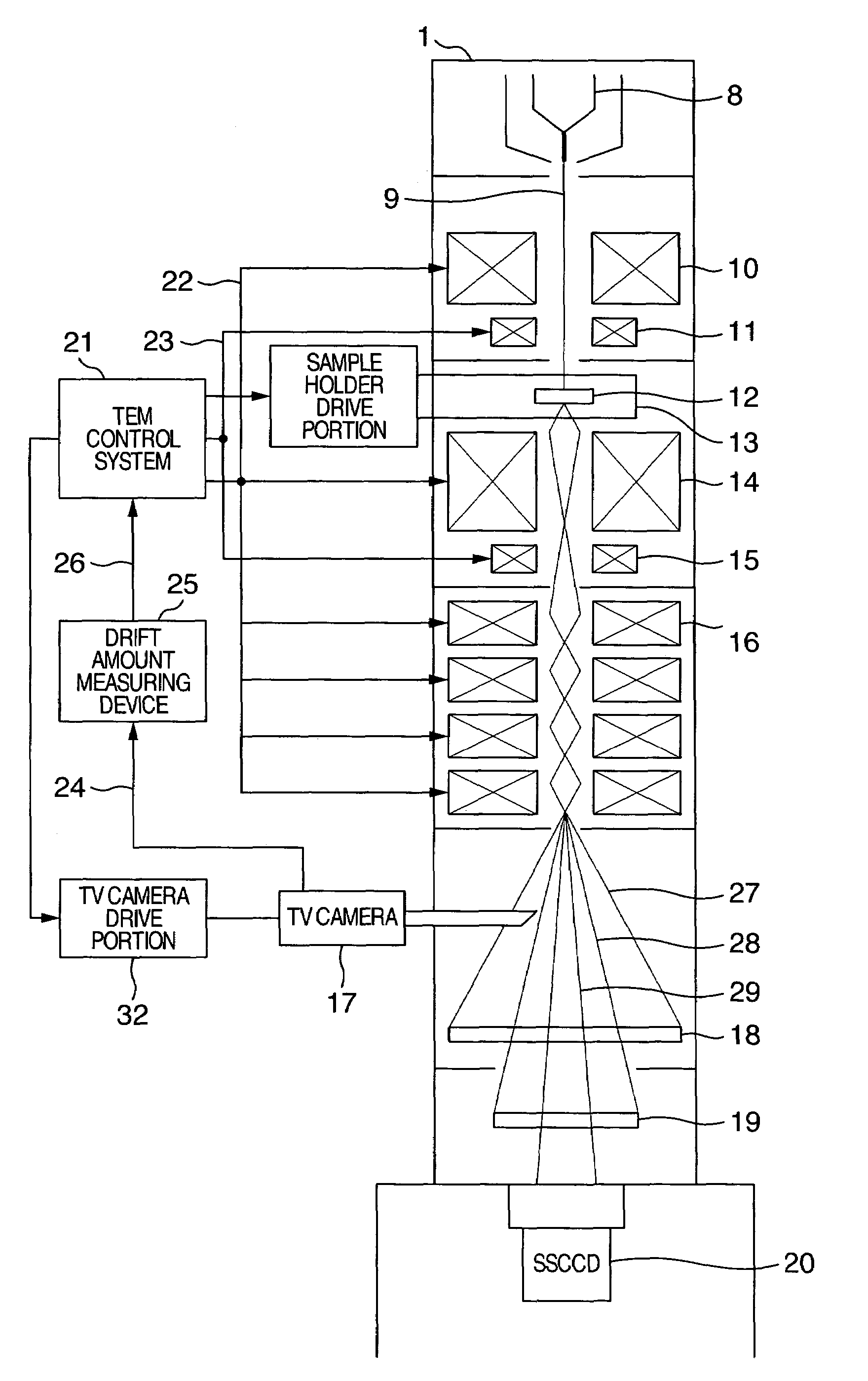
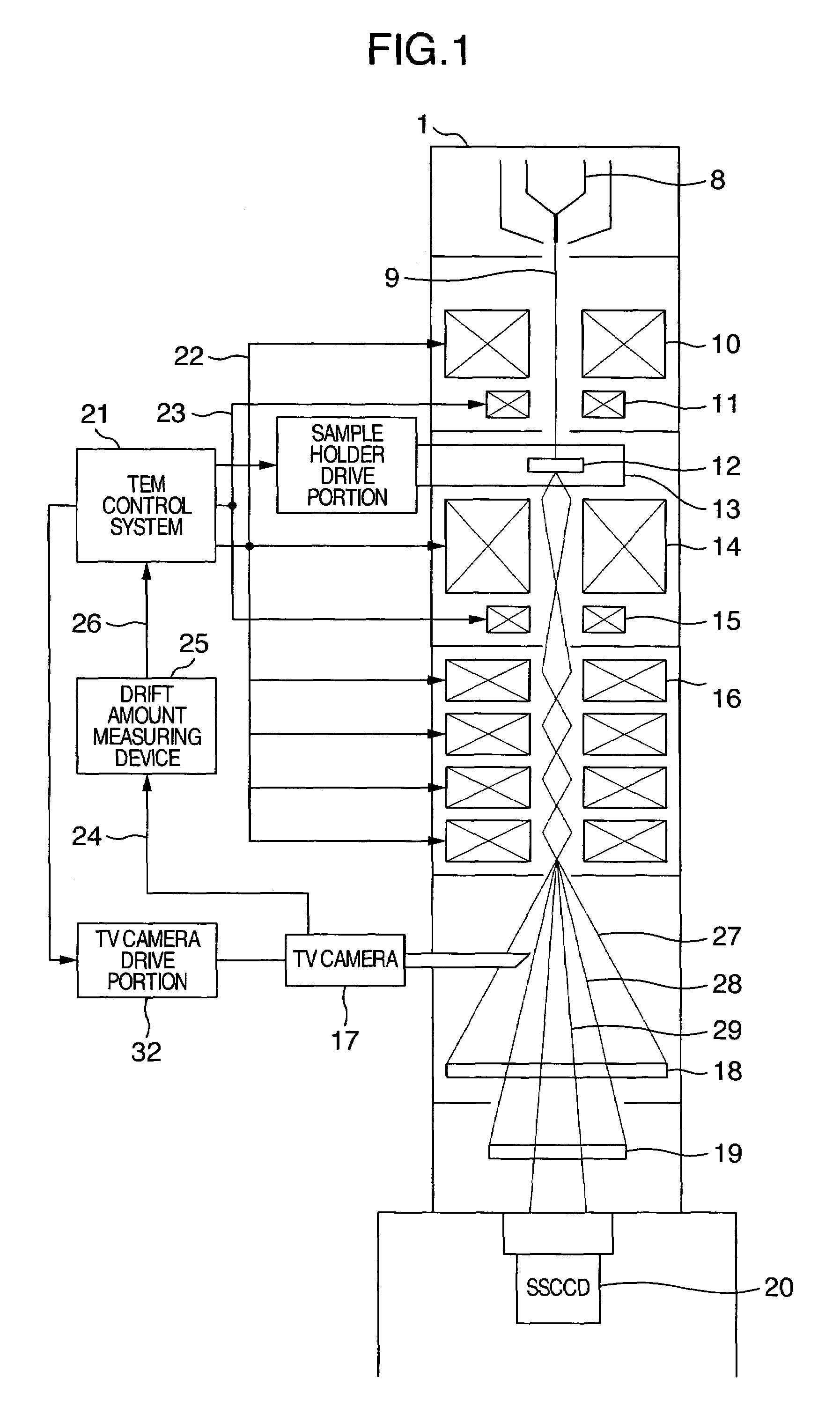
[0025]FIG. 1 is a block diagram showing a transmission electron microscope according to the invention. An electron beam 9 generated in an electron gun 8 is applied onto a specimen 12 by a converging lens 10. The position and angle of irradiation can be adjusted by a deflection coil 11. A transmission electron image of the specimen 12 is magnified by an objective lens 14 and intermediate / projection lenses 16, so that the transmission electron image can be observed on an observation fluorescent screen 18. The specimen 12 to be observed is fixed into a specimen holder 13, so that the view field of observation can be adjusted by movement of the specimen holder 13. If an image shift coil 15 is used, the view field of observation can be adjusted electromagnetically without movement of the specimen holder 13. A TEM control system 21 controls all lens systems, electron beam deflection systems and specimen manipulation systems.
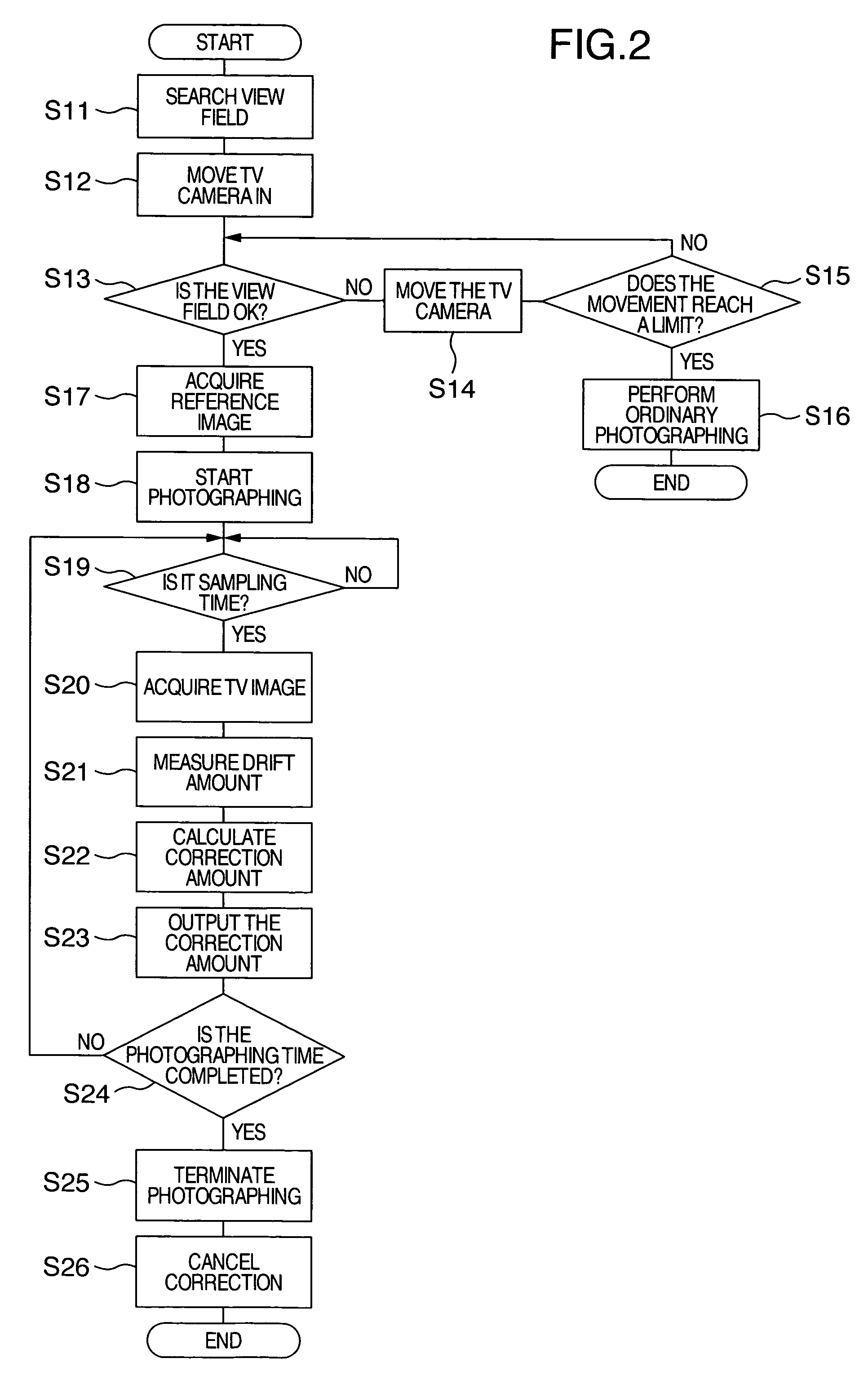
[0026]The view field 27 of the observation fluorescent screen is ...
second embodiment
[0034]A method using the second embodiment for recording a TEM image not affected by drift will be described with reference to FIG. 4 which is a flow chart showing a specific procedure. First, the view field of observation is searched (S31) so that a specimen is moved into the view field 28 of the photographic film or the view field 29 of the SSCCD. Then, the PSD 30 is inserted in a region of the view field 27 of the observation fluorescent screen except the view field 28 of the photographic film and the view field 29 of the SSCCD (S32). When the PSD 30 is located out of view field in which drift can be detected, for example, when the PSD 30 is in the place where the specimen is not provided or in a portion of a mesh frame, the voltage signal from the PSD becomes unstable or comes out of the center of the voltage range. In such a case (S33), the PSD 30 is moved by the PSD drive portion 33 (S34) so that the output voltage comes to the nearly center of the voltage range stably. If the...
PUM
| Property | Measurement | Unit |
|---|---|---|
| frequency | aaaaa | aaaaa |
| rise time | aaaaa | aaaaa |
| transmission electron microscope | aaaaa | aaaaa |
Abstract
Description
Claims
Application Information


