Die-level process monitor and method

a process monitor and die-level technology, applied in semiconductor/solid-state device testing/measurement, semiconductor/solid-state device details, instruments, etc., can solve the problems of large area of silicon wafers, devoted test, and inability to ship out dies as products to customers, etc., to reduce the footprint of dlpm, reduce the size of the package, and reduce the area available for i

Inactive Publication Date: 2007-07-03
RIDGETOP GROUP
View PDF16 Cites 43 Cited by
  • Summary
  • Abstract
  • Description
  • Claims
  • Application Information

AI Technical Summary

Benefits of technology

[0013]Since the DLPM is preferably added to each die, it is desirable to minimize the DLPM's footprint to keep the size of the package small and the area available for the IC as large as possible. The pads for performing I/O between the DLPM and the outside world typically dominate the size of the package, and thus it is desirable to minimize their use. In an embodiment, any external c

Problems solved by technology

In spite of strictly governed foundries, semiconductor processing inevitably yields a distribution of parameter values.
The foundry's test structure designs consume large areas of the silicon wafer, require many area-consuming pads for I/O, require external equipment including a probe station, controllable/programmable voltage supply, current meter, ohm meter, volt meter, etc. to perform I/O, and are destroyed and rendered useless during the dicing process.
A foundry may designate an entire wafer or specific die sites for testing and not destroy the test structures, ho

Method used


Image

  • Die-level process monitor and method
  • Die-level process monitor and method
  • Die-level process monitor and method

Examples


Embodiment Construction

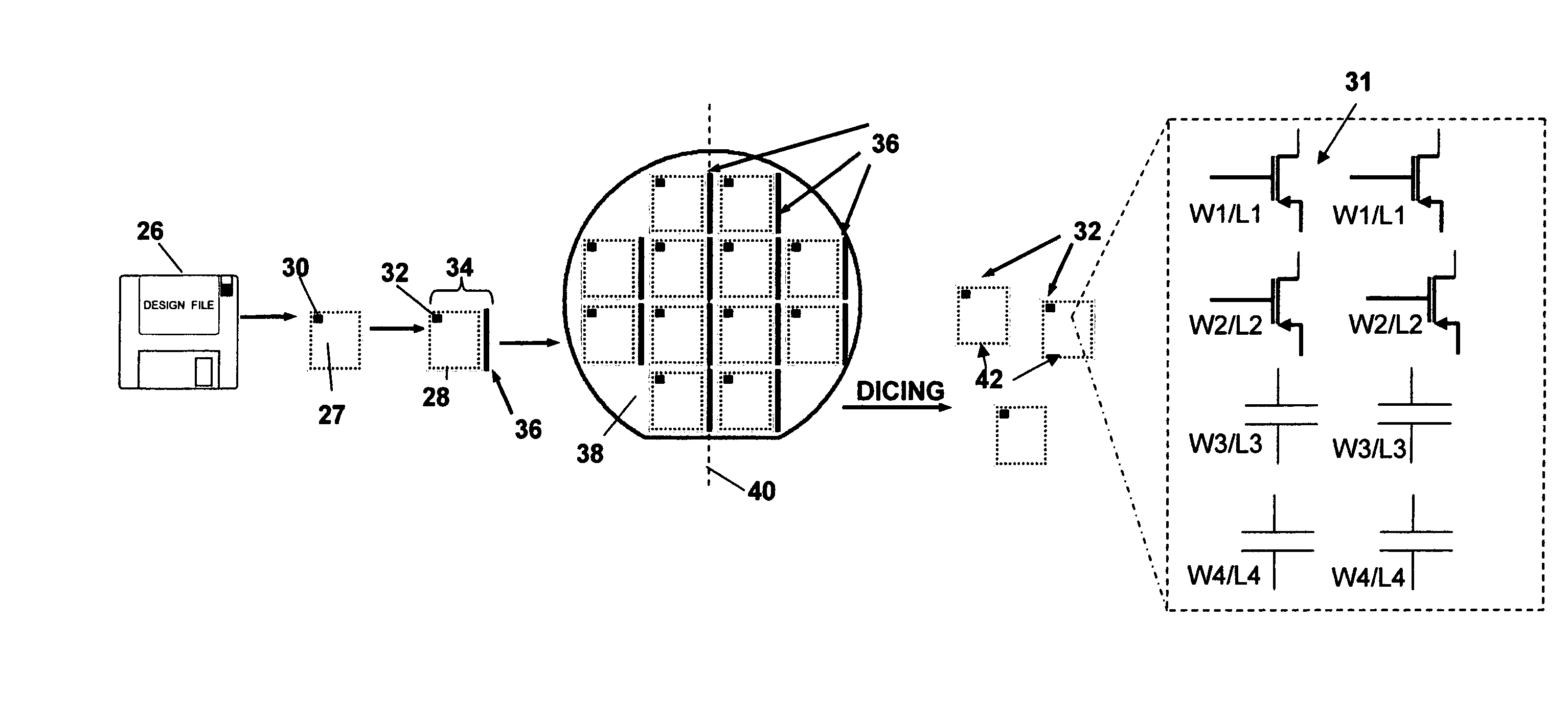
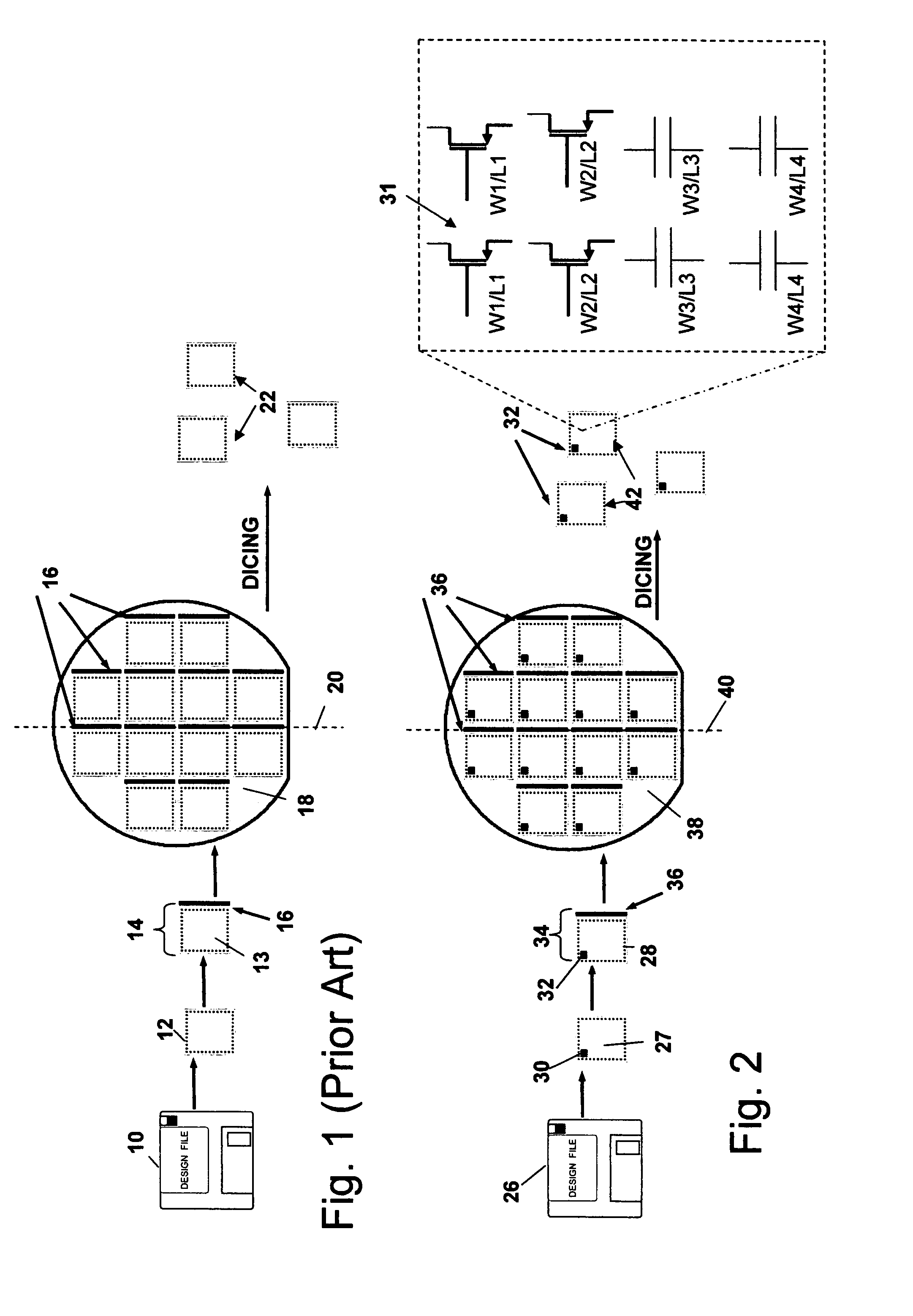
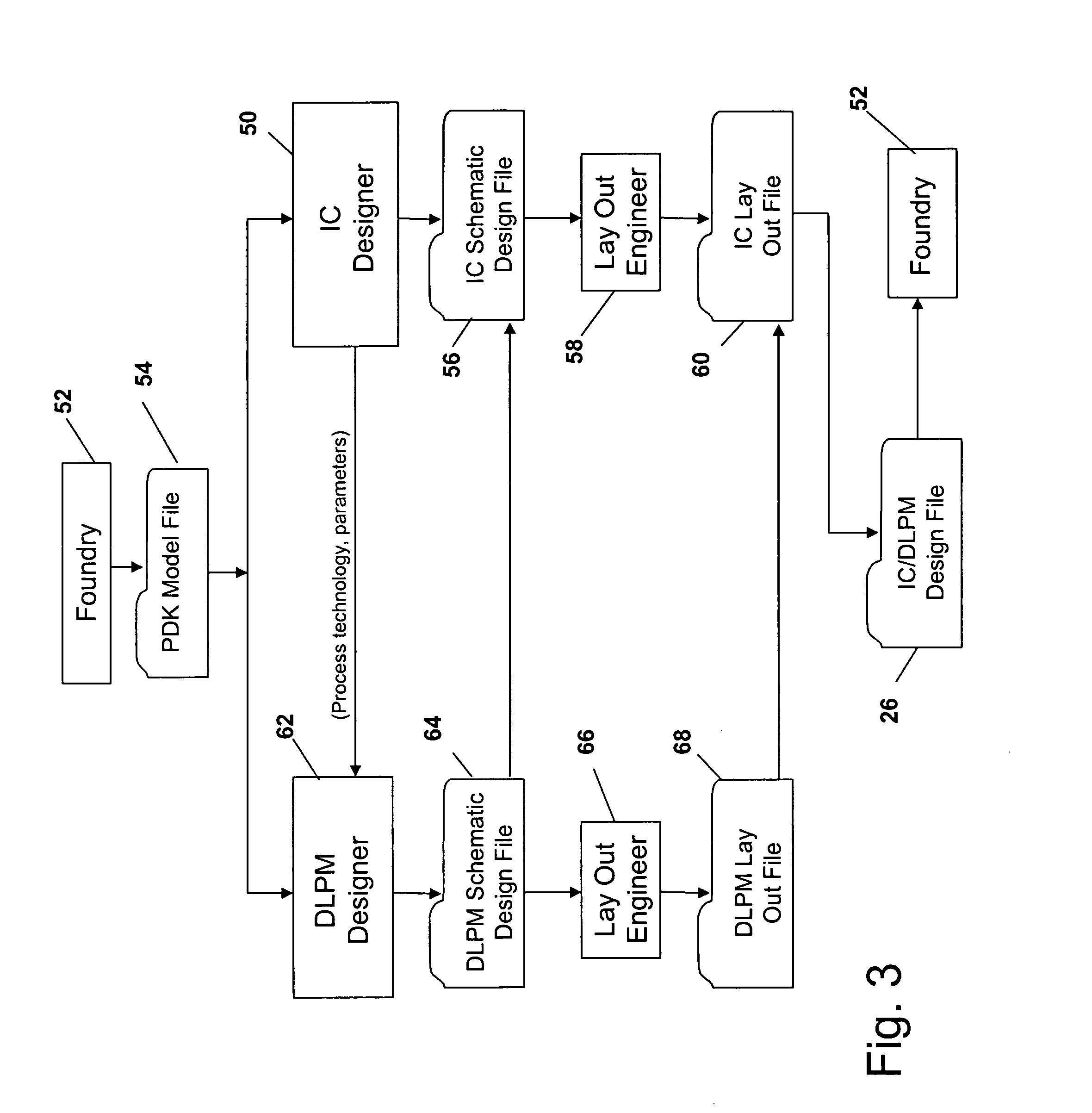
[0025]The present invention provides a die-level process monitor (DLPM) to verify whether semiconductor processing-related parameters are within specified design limits and to accumulate statistics thereof. A process monitor small enough to be implemented at the die level is instrumental to determine root causes of circuit malfunctions and reliability issues. The DLPM will aid process and circuit engineers to extract both process parameters (transistor threshold voltage, resistance, capacitance and inductance, transconductance, output conductance) and respective statistical variations. The DLPM may also be used by the IC to adjust bias conditions based on feedback from the DLPM.

[0026]Semiconductor die contain an integrated circuit that performs an electronic function. Although thousands of electronic devices compose the IC, a large portion of this quantity is made up of identical devices. These devices are necessarily designed identically to ensure desired circuit performance. Due t...


PUM


Abstract

A die-level process monitor (DLPM) provides a means for independently determining whether an IC malfunction is a result of the design or the manufacturing processing and further for gathering data on specific process parameters. The DLPM senses parameter variations that result from manufacturing process drift and outputs a measure of the process parameter. The DLPM will typically sense the mismatch of process parameters between two or more test devices as a measure of process variation between a like pair of production devices. The DLPM may be used as a diagnostic tool to determine why an IC failed to perform within specification or to gather statistics on measured process parameters for a given foundry or process.

Description

CROSS-REFERENCE TO RELATED APPLICATIONS[0001]This application claims benefit of priority under 35 U.S.C. 119(e) to U.S. Provisional Application No. 60 / 581,811 entitled “Die-Level IC Process Monitor Method and Apparatus” filed on Jun. 23, 2004, the entire contents of which are incorporated by reference.BACKGROUND OF THE INVENTION[0002]1. Field of the Invention[0003]This invention relates to process monitors for semiconductor fabrication and more specifically to a die-level process monitor (DLPM).[0004]2. Description of the Related Art[0005]Variations of device parameters such as transistor threshold voltage, resistance, capacitance, inductance, transconductance, and output conductance are certain to occur due to the complexity of semiconductor processing, involving energy, temperature, pressure and concentration gradients as well as geometrical and cleanliness requirements. In spite of strictly governed foundries, semiconductor processing inevitably yields a distribution of parameter...

Claims


Application Information

Patent Timeline
IPC IPC(8): G01R31/02
CPCG01R31/2884
Inventor RALSTON-GOOD, JEREMY JOHNSPUHLER, PHILIPP S.VERMEIRE, BERT M.GOODMAN, DOUGLAS LEONARD
Owner RIDGETOP GROUP
Why Eureka
Try Eureka