Optical reduction system with control of illumination polarization

Inactive Publication Date: 2007-07-03
ASML HLDG NV
View PDF12 Cites 59 Cited by
  • Summary
  • Abstract
  • Description
  • Claims
  • Application Information

AI Technical Summary

Benefits of technology

[0007]While these optical systems perform adequately for their intended purpose, there is an ever increasing need to improve system performance. The present inventor has identified that a need exists

Problems solved by technology

The introduction of compensation to control illumination polarization limits the performance impact of reticle birefringence on polarization sensitive projection optics including catadioptric projection optic.
This change alters the performance of the entire system.
This leads to dose errors at the wafer.
Dose errors contrib

Method used


Image

  • Optical reduction system with control of illumination polarization
  • Optical reduction system with control of illumination polarization
  • Optical reduction system with control of illumination polarization

Examples


example implementations

V. Example Implementations

[0076]A. Optical System with Control of Laser Illumination Polarization

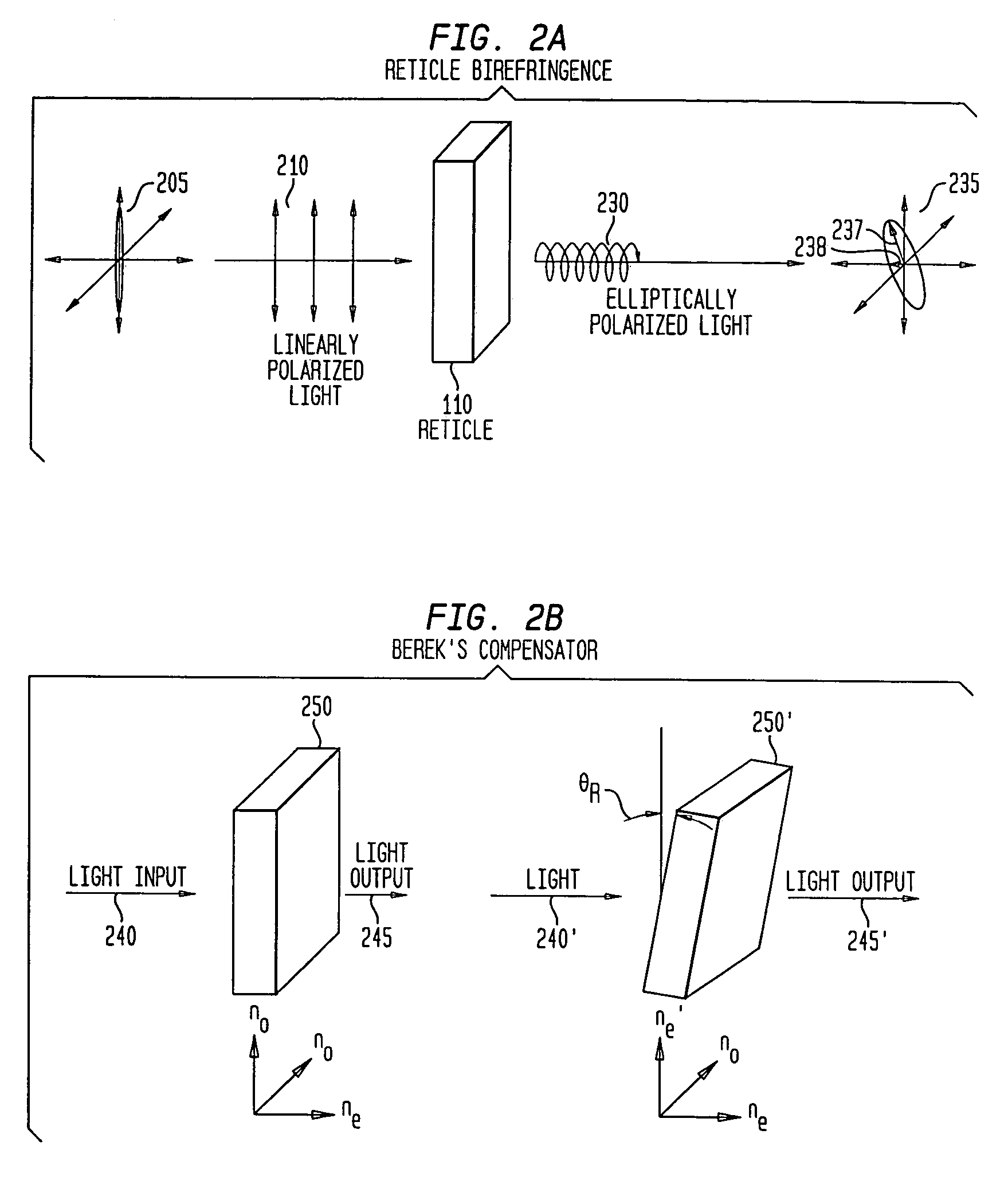
[0077]The present invention uses variable wave plates to minimize dose errors in a polarization sensitive projection optic system caused by the variation of birefringence over the reticle. As described with respect to the figures, a single polarization compensator provides a single correction for the entire reticle. In one embodiment, multiple complex correctors can provide a correction that varies as a function of reticle position.

[0078]In another embodiment, the compensator system can be designed to offset the illumination polarization to compensate for local reticle birefringence.

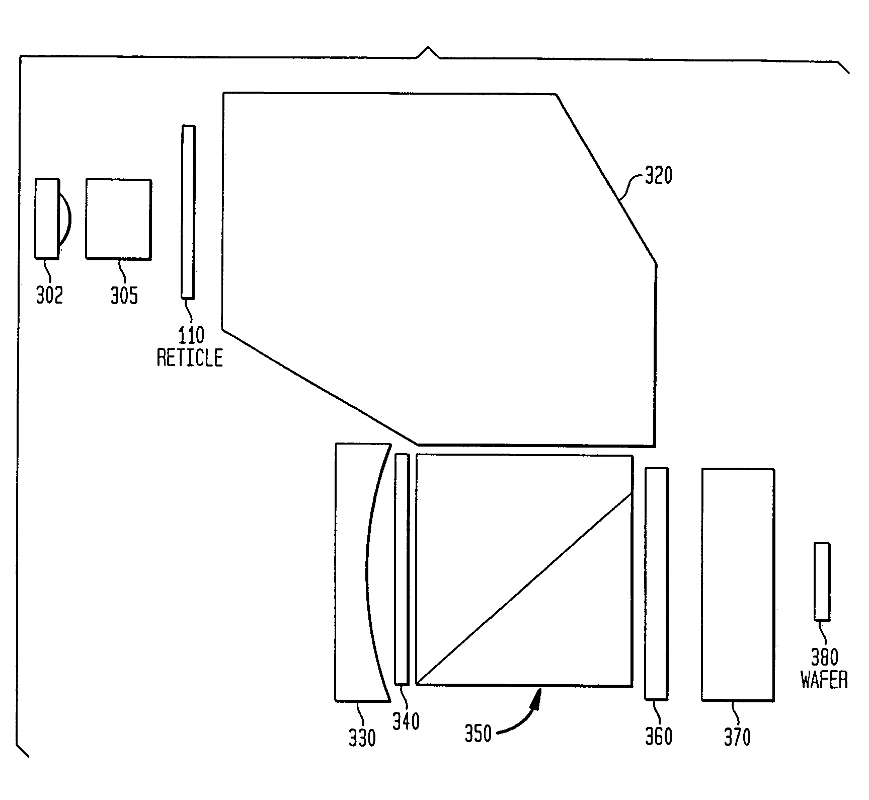
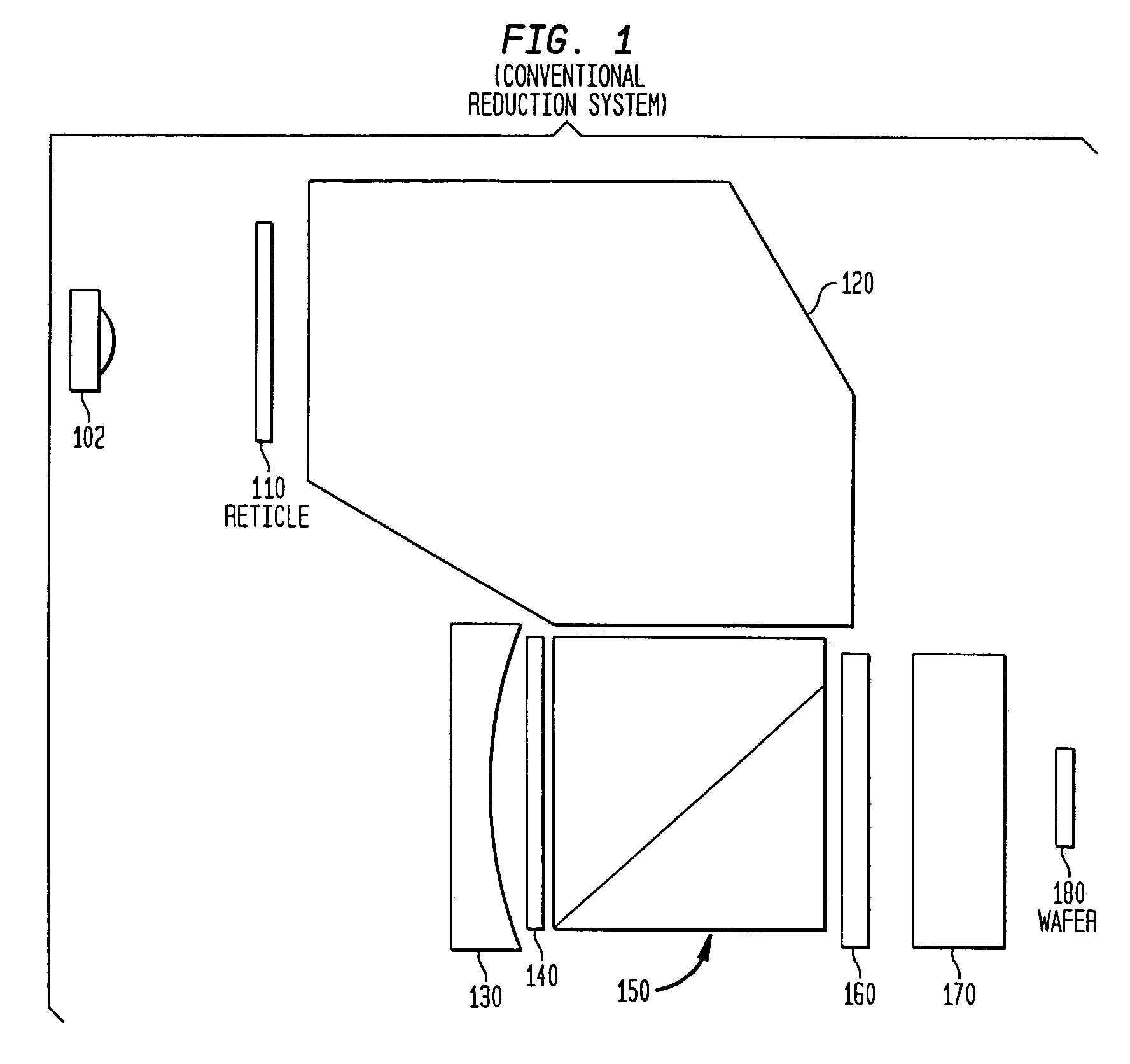
[0079]In one embodiment, for dose control, the polarization state can be evaluated over the exposure. For example, the polarization state can be averaged over the reticle. FIG. 3 illustrates an embodiment of the present invention that eliminates such asymmetries or print biases. FIG. 3 shows a first optical c...


PUM


Abstract

An optical reduction system with polarization dose sensitive output for use in the photolithographic manufacture of semiconductor devices having variable compensation for reticle retardation before the long conjugate end. The variable compensation component(s) before the reticle provides accurate adjustment of the polarization state at or near the reticle. The variable compensation components can be variable wave plates, layered wave plates, opposing mirrors, a Berek's compensator and/or a Soleil-Babinet compensator. The catadioptric optical reduction system provides a relatively high numerical aperture of 0.7 capable of patterning features smaller than 0.25 microns over a 26 mm×5 mm field. The optical reduction system is thereby well adapted to a step and scan microlithographic exposure tool as used in semiconductor manufacturing. Several other embodiments combine elements of different refracting power to widen the spectral bandwidth which can be achieved.

Description

CROSS-REFERENCE TO RELATED APPLICATIONS[0001]This application is a continuation of U.S. Ser. No. 09 / 841,185, filed Apr. 25, 2001 (now U.S. Pat. No. 6,680,798 that issued Jan. 20, 2004), which claimed benefit under 35 U.S.C. § 119(e) to U.S. Prov. App. No. 60 / 199,381, filed Apr. 25, 2000, which are both incorporated by reference herein in their entireties.BACKGROUND OF THE INVENTION[0002]1. Field of the Invention[0003]This invention relates generally to optical systems used in semiconductor manufacturing[0004]2. Related Art[0005]Semiconductor devices are typically manufactured using various photolithographic techniques. The circuitry used in a semiconductor chip is projected from a reticle onto a wafer. This projection is often accomplished with the use of optical systems. The design of these optical systems is often complex, and it is difficult to obtain the desired resolution necessary for reproducing the ever-decreasing size of components being placed on a semiconductor chip. Ther...

Claims


Application Information

Patent Timeline
IPC IPC(8): G02B27/28G02B5/30G02B17/08G02B27/18G03F7/20G03F7/22H01L21/027
CPCG02B5/3083G02B17/08G02B17/0892G02B27/286G03F7/70225G03F7/70358G03F7/70566G03F7/70966H01L21/027
Inventor KREUZER, JUSTIN L.
Owner ASML HLDG NV
Why Eureka
Try Eureka