Semiconductor structure

a technology of semiconductors and semiconductors, applied in the direction of semiconductor devices, electrical devices, transistors, etc., can solve the problems of increasing the capacitance of the device (at the junction) affecting circuit performance, increasing the difficulty of increasing the doping in specific areas, and preventing the latch-up of the device. the effect of preventing the devi

Inactive Publication Date: 2007-07-10
TAIWAN SEMICON MFG CO LTD
View PDF14 Cites 28 Cited by
  • Summary
  • Abstract
  • Description
  • Claims
  • Application Information

AI Technical Summary

Benefits of technology

[0007]In a first aspect of the invention, a structure comprises a “deep sub-collector” (DS) located in a first epitaxial layer and a “near sub-collector” (NS) located in a second epitaxial layer. The structure further comprises a deep trench (DT) isolation structure isolating a region which is substantially above the deep sub-collector, a reach-through structure in contact with the near sub-collector, and a reach-through structure in contact with the deep sub-collector to provide a low-resistance shunt, which prevents latch-up of a device.
[0010]The invention also provides for a structure comprising a deep sub-collector located in a first epitaxial layer, a near sub-collector located in a second epitaxial layer, a deep trench isolation structure isolating a region which is substantially above the deep sub-collector, a reach-through structure in contact with the near sub-collector, and a reach-through structure in contact with the deep sub-collector to provide a low-resistance shunt, which prevents latch-up of a device.

Problems solved by technology

However, in CMOS structures, parasitic current paths exist associated by so-called parasitic bipolar transistors, which, under normal conditions, are not activated.
Thus, due to the scaling, previous techniques to prevent CMOS latch-up are becoming more problematic.
For example, it is more difficult to increase the doping in specific areas, since the increase in dopants will increase the out-diffusion of the dopants which, in turn, increases the capacitance of the device (at the junctions) impacting circuit performance.

Method used


Image

  • Semiconductor structure
  • Semiconductor structure
  • Semiconductor structure

Examples


Embodiment Construction

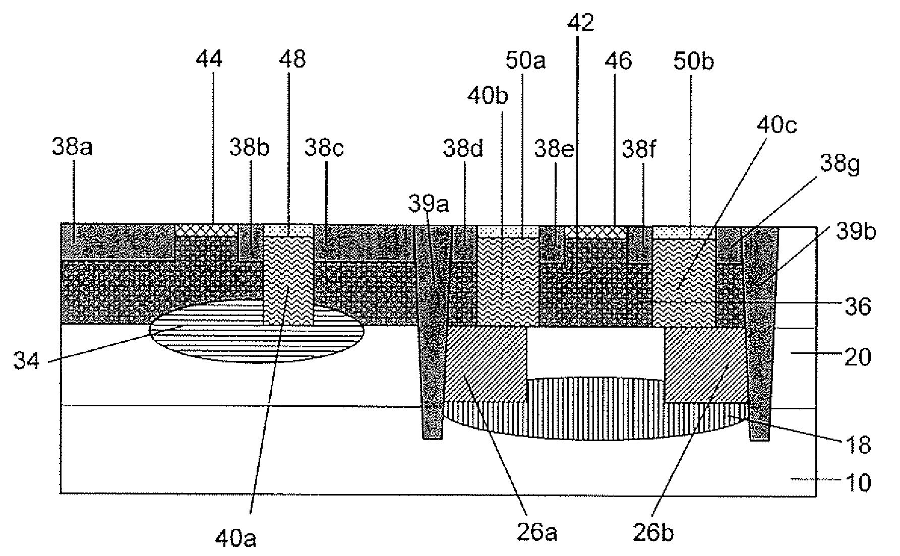
[0019]The invention relates to a semiconductor structure and a method of manufacturing. In embodiments, the invention more specifically relates to a method of manufacture forming a double epitaxy / double sub-collector triple-well structure. In embodiments, the processing steps implemented by the invention minimize P+ / N+ space, while preventing CMOS latch-up, e.g., prevents the structure going from a low current / high voltage state to a high current / low voltage state. The invention may be suitable for CMOS, RF CMOS, BiCMOS, RF BiCMOS, RF BiCMOS Silicon Germanium (SiGe), RF BiCMOS Silicon Germanium Carbon (SiGeC), bipolar SOI, homo-junction, and heterojunction bipolar transistor (HBT) devices, to name a few. (U.S. application Ser. No. 11 / 163,882 is herein incorporated by reference in its entirety.)

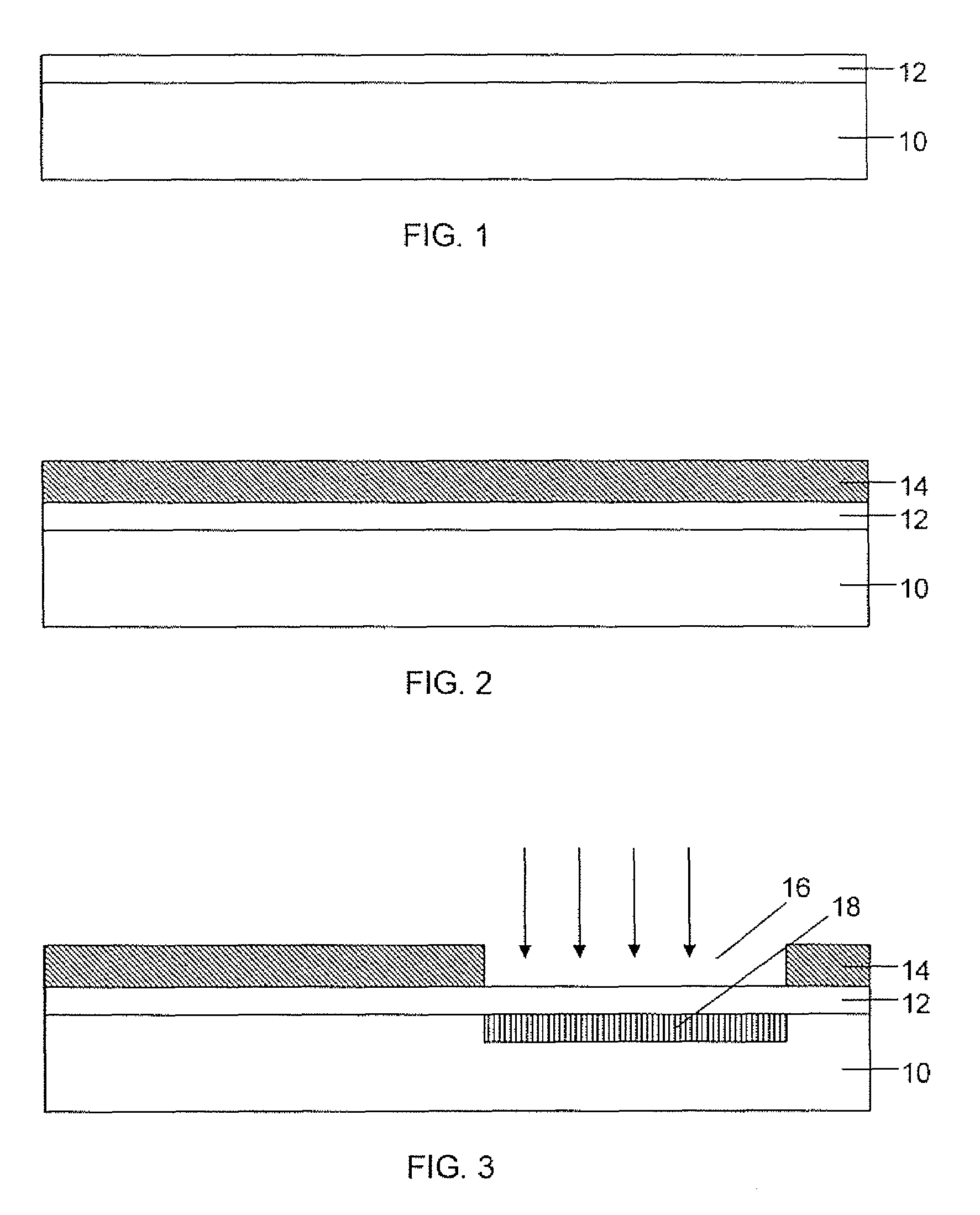
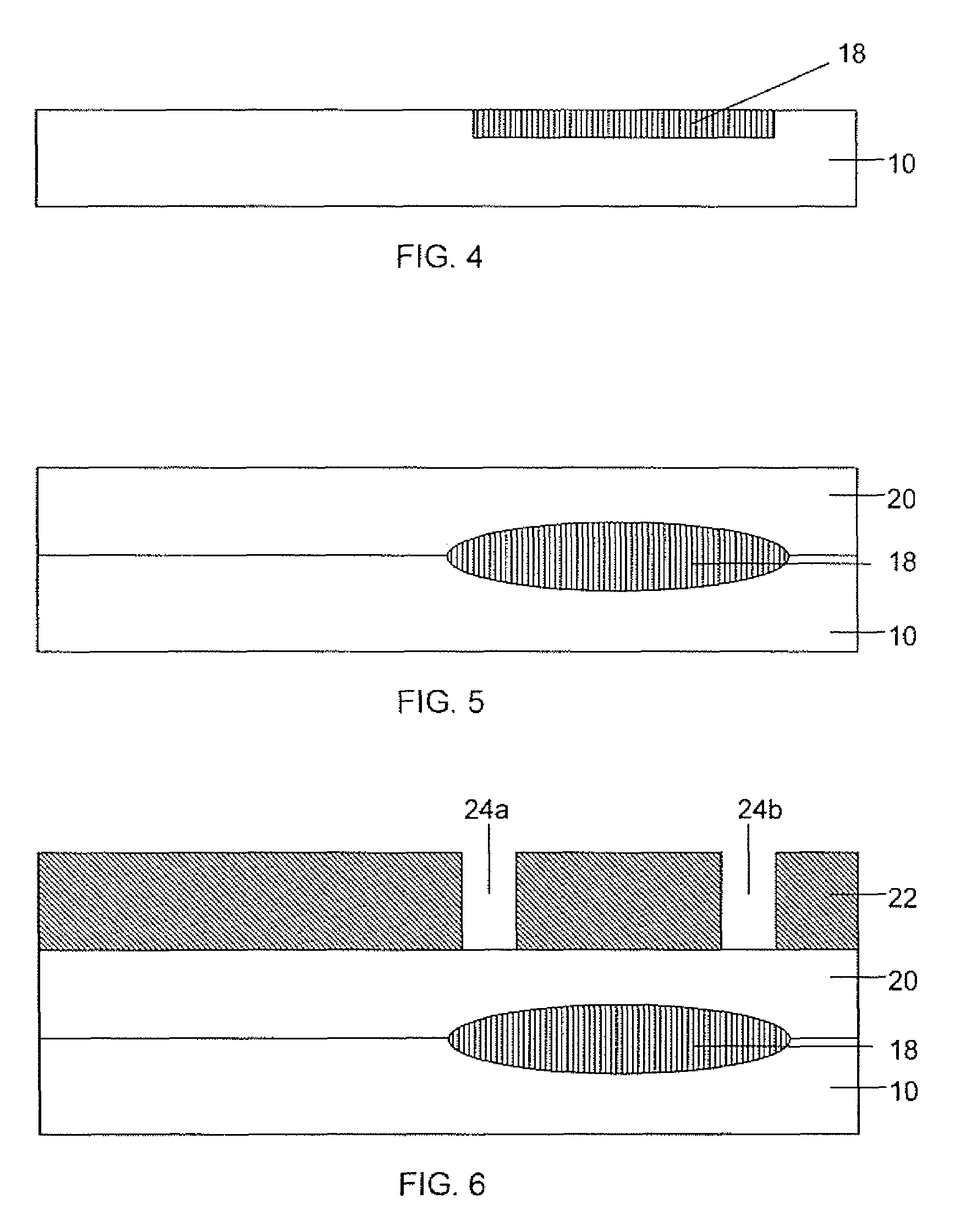
[0020]Referring to FIG. 1, a starting structure is shown, which includes a substrate 10. In one embodiment, the substrate may be silicon, or germanium although other materials and / or substrate...


PUM


Abstract

A structure comprises a deep sub-collector buried in a first epitaxial layer and a near sub-collector buried in a second epitaxial layer. The structure further comprises a deep trench isolation structure isolating a region which is substantially above the deep sub-collector, a reach-through structure in contact with the near sub-collector, and a reach-through structure in contact with the deep sub-collector to provide a low-resistance shunt, which prevents COMS latch-up of a device. The method includes forming a merged triple well double epitaxy / double sub-collector structure.

Description

FIELD OF THE INVENTION[0001]The invention relates generally to a semiconductor structure and method of manufacturing and more particularly to a merged triple well double epitaxy / double sub-collector structure.BACKGROUND OF THE INVENTION[0002]CMOS (complementary metal oxide semiconductor) circuits are widely used in many applications such as, for example, battery-powered devices such as portable computers and cellular telephones. CMOS is a very effective device configuration for implementation of digital functions due to very low power consumption and dissipation as well minimization of the current in the “off” state.[0003]In implementation, CMOS semiconductors comprise both n-channel and p-channel MOS field effect transistors (MOSFETs), i.e., use both n-channel MOSFETs, and p-channel MOSFETs. However, in CMOS structures, parasitic current paths exist associated by so-called parasitic bipolar transistors, which, under normal conditions, are not activated. CMOS latch-up can occur when...

Claims


Application Information

Patent Timeline
Patent Type & Authority Patents(United States)
IPC IPC(8): H01L29/00
CPCH01L21/823892H01L27/0623H01L27/0921
Inventor LIU, XUEFENGRASSEL, ROBERT M.VOLDMAN, STEVEN H.
Owner TAIWAN SEMICON MFG CO LTD
Why Eureka
Try Eureka