Field-effect transistor structure and associated semiconductor memory cell

a field-effect transistor and memory cell technology, applied in transistors, semiconductor devices, electrical apparatus, etc., can solve the problems of rapid and effective dissipation of charge carriers, electrical properties remain uninfluenced, etc., and achieve the effect of dissipation of excess charge carriers and prevention of body effects

Inactive Publication Date: 2007-07-31
INFINEON TECH AG
View PDF4 Cites 14 Cited by
  • Summary
  • Abstract
  • Description
  • Claims
  • Application Information

AI Technical Summary

Benefits of technology

[0018]In particular, a diode doping region permits realization of a diode in the semiconductor substrate and a diode connection layer which is electrically conductively connected to a control layer of the field-effect transistor structure permits dissipation of excess charge carriers in the semiconductor substrate. This prevent body effects since the body potential is upwardly limited by the diode voltage.
[0019]A depression is formed in the semiconductor substrate, the diode doping region being formed in the bottom region of the depression and the diode connection layer being formed at least in partial regions of the depression. In this way, it is possible to arrange the diode for dissipating excess charge carriers in an optimum depth of the semiconductor substrate, as a result of which the electrical properties of the field-effect transistor structure remain uninfluenced to a particular degree. The depression is formed, for example, directly beside a channel region in a shallow trench isolation that defines a channel width of the channel region, thus resulting in a space-optimized realization which is suitable for high integration densities.
[0020]A dielectric layer is formed at the walls of the depression between the diode connection layer and the semiconductor substrate for the purpose of realizing a capacitor connected to the control layer, thereby enabling not only the limitation of the body potential by the diode but also an intensified dynamic coupling of the control layer to the body or the semiconductor substrate. In particular in the case of frequently changing signals at the control layer, this results in rapid and effective dissipation of charge carriers, as a result of which the electrical properties remain uninfluenced to a particular degree.
[0021]When using a highly doped semiconductor material as a diode connection layer, it is possible, on account of outdiffusion during later thermal process steps, to form the diode doping region without an additional process step and in a self-aligning manner in the semiconductor substrate, thereby significantly simplifying the requirements made of an alignment accuracy.
[0022]A semiconductor memory cell having a selection transistor of the type described above is connected to a trench capacitor by its first source / drain region and to a bit line by its second source / drain region, the control layer constituting a part of a word line running essentially perpendicular to the bit line, and the diode doping region being formed below the word line in the semiconductor substrate. In the case of an arrangement of this type, a self-aligning contact connection between the control layer and the diode doping region is obtained in a particularly simple manner.
[0026]With regard to the method for fabricating a semiconductor structure, a semiconductor substrate is prepared in a suitable manner, a depression is formed in a trench isolation, a diode doping region is formed at the bottom of the depression and an electrically conductive diode connection layer is filled in the depression, a mask layer is removed, a gate insulation layer is formed, a control layer is formed at the surface of the gate insulation layer, the surface thus fabricated is planarized at least as far as the trench isolation and an electrically conductive connecting layer is subsequently formed for the purpose of connecting the control layer to the diode connection layer. In this way, it is possible to adapt standard processes with minimal changes or insertions of additional process steps for the realization of the above-described diode doping regions and diode connection layers. This results in a particularly simple and cost-effective realization.

Problems solved by technology

In particular in the case of frequently changing signals at the control layer, this results in rapid and effective dissipation of charge carriers, as a result of which the electrical properties remain uninfluenced to a particular degree.

Method used


Image

  • Field-effect transistor structure and associated semiconductor memory cell
  • Field-effect transistor structure and associated semiconductor memory cell
  • Field-effect transistor structure and associated semiconductor memory cell

Examples


Embodiment Construction

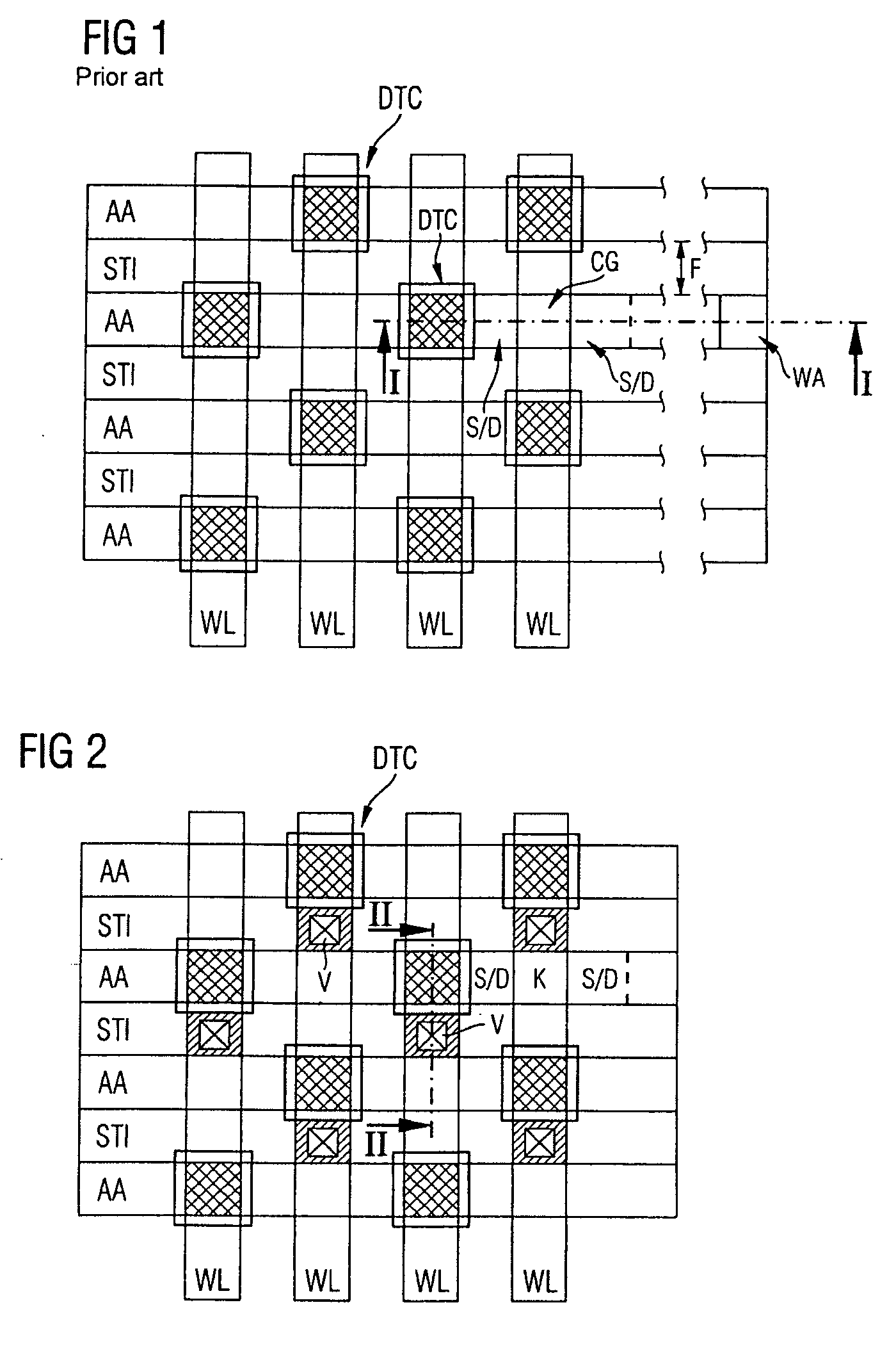
[0039]FIG. 2 shows a simplified plan view of a semiconductor memory cell arrangement in accordance with a first exemplary embodiment, identical reference symbols representing elements and layers identical or corresponding to those in FIG. 1 and a repeated description being dispensed with below.

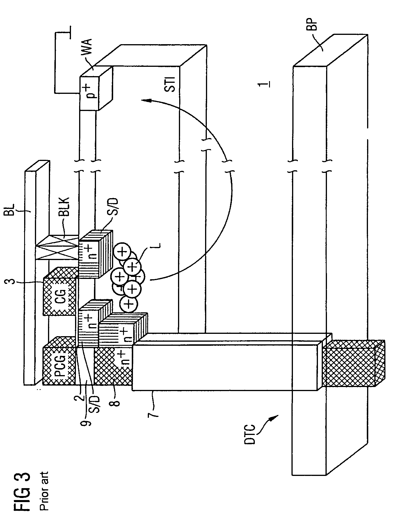
[0040]The perspective view along a section I-I in FIG. 1 which is illustrated in FIG. 3 in this case also essentially corresponds to a corresponding section (not illustrated) in FIG. 2, but the well connection doping region WA may not be present in the exemplary embodiment according to the invention. In accordance with FIG. 2, the well connection doping region, which is no longer effective on account of increased packing densities, is replaced by a depression V, which is formed in a shallow trench isolation STI and at the bottom region of which a diode doping region is formed in the semiconductor substrate.

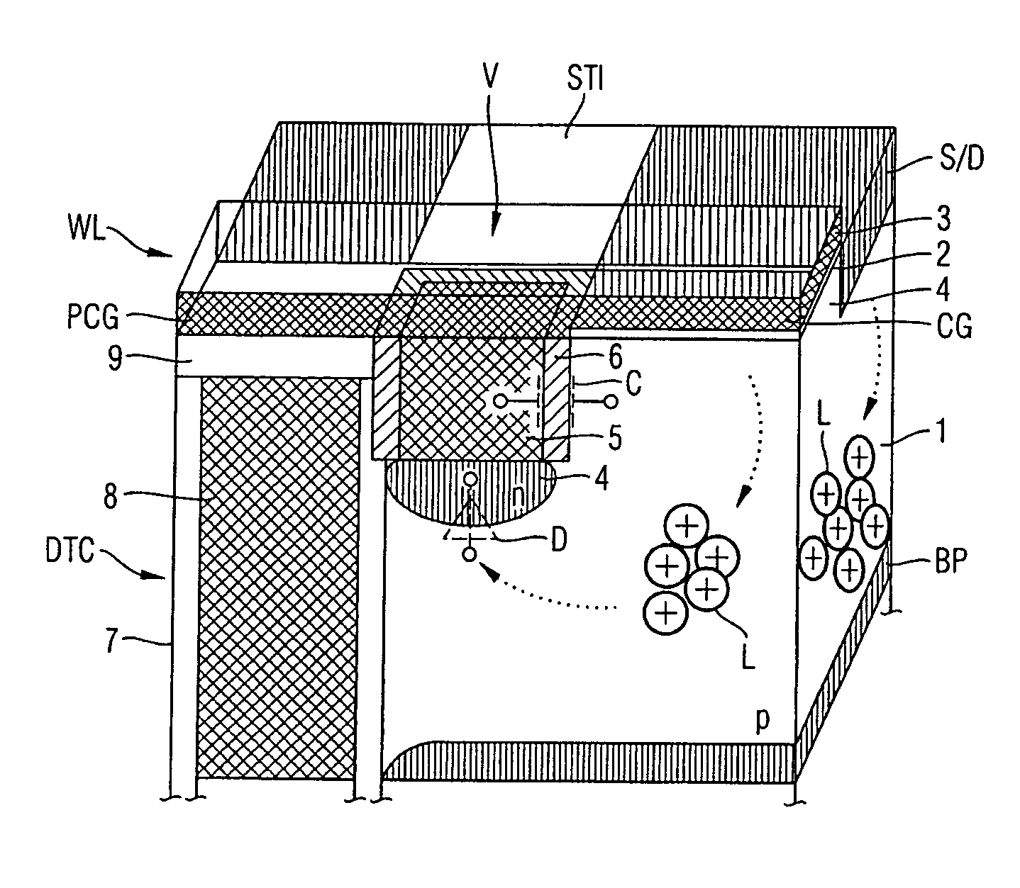
[0041]FIG. 5 shows a simplified perspective view of the semiconductor memory cell accord...


PUM


Abstract

A field-effect transistor (FET) structure and method of formation thereof is presented. The FET structure includes first and second source / drain regions formed in a semiconductor substrate to define a channel region. A gate insulation layer is formed at a surface of the channel region. A control layer is formed at a surface of the gate insulation layer. A diode doping region is formed to realize a diode in the semiconductor substrate. An electrically conductive diode connection layer connects the diode doping region to the control layer. A depression is formed in the semiconductor substrate. The diode doping region is formed at a bottom of the depression and the diode connection layer is formed in the depression to dissipate excess charge carriers in the semiconductor substrate.

Description

PRIORITY[0001]This application is a continuation of International Application PCT / DE03 / 003748, filed on Nov. 12, 2003, which claims the benefit of priority to German Patent Application 102 54 415.8, filed on Nov. 21, 2002, incorporated herein by referenceTECHNICAL FIELD[0002]The present invention relates to a field-effect transistor structure, an associated semiconductor memory cell and an associated fabrication method, and in particular to a field-effect transistor structure as can be used in DRAM memories.BACKGROUND[0003]In semiconductor technology, the most advanced technologies with the highest integration densities are used in particular for fabricating so-called DRAM memories (dynamic random access memory). With an increasing packing density or integration density, however, the following difficulties result for example in DRAM semiconductor memories:[0004]In order to control a short-channel behavior (roll-off) of a selection transistor in a DRAM semiconductor memory cell, from...

Claims


Application Information

Patent Timeline
Patent Type & Authority Patents(United States)
IPC IPC(8): H01L27/108H01L29/76H01L29/94H01L31/119H01L21/8242H01L27/02
CPCH01L27/10861H01L27/10891H01L27/0214H01L27/108H01L27/10873H10B12/038H10B12/05H10B12/00H10B12/488
Inventor HIERLEMANN, MATTHIASSTRASSER, RUDOLF
Owner INFINEON TECH AG
Why Eureka
Try Eureka