[0009]There is a need in the art in a novel photoelectric structure enabling maximum utilization of the
semiconductor materials. Such need is associated with the following: The main drawback of the known photoelectric devices (e.g.
solid state solar cells and photodiodes) is associated with their high cost, relative to the
fossil fuel cost (3-6 $ / W generation cost for a
solar cell system, vs. 1 $ / W generation cost for a
fossil fuel system). Also, the conversion efficiencies of conventional solar cell systems are quite low, i.e. about 10%-17%. Moreover, the effectivity of conventional photoelectric devices is highly dependent on the temperature conditions of the environment which increases the effects of charge carriers recombination mechanisms (such as surface state recombination and Shockley Reed Hall (SRH) recombination), thus reducing the device efficiency with the increase in its operational temperature.
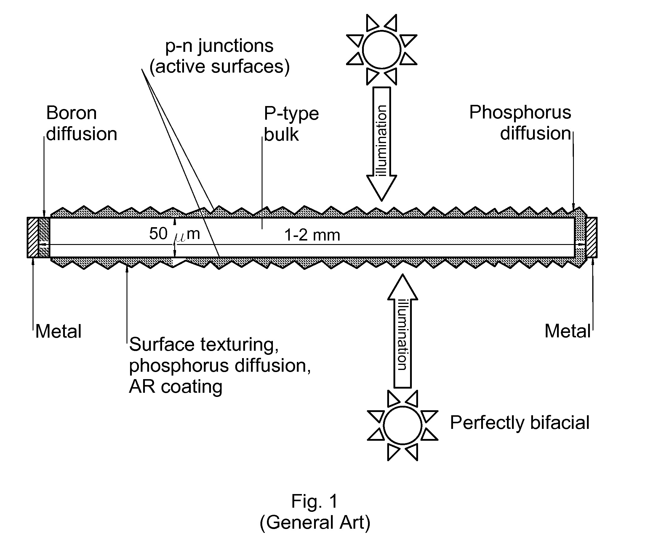
[0011]The
depletion region at the interface between the different-type
conductivity layers has
high resistivity since all of the free charged carriers leave this region due to the built-in
electric field at the junction. This
high resistivity leads to an increase in the probability of charge carriers' generation. Propagation of these charge carriers through multiple
layers of different
conductivity properties (e.g. different structures) and through interfaces between them increases effects of recombination processes associated with such mechanisms as surface state recombination, and crystalline defects namely trap recombination (Shockley-Reed-Hall recombination). This leads to reduction in the
photoelectric conversion efficiency, of the conventional (namely vertical) photovoltaic structures and photodiodes in which the charge carriers, generated within the
depletion region, propagate across the junction of different conductivity type structures.
[0012]Also, as noted above, the efficiency of a conventional photovoltaic device is highly influenced by the temperature of the device. Increasing the temperature leads to an increase in the intrinsic charge carriers concentration ni (proportional to T3 / 2exp(−Eg / 2 kT), T being the temperature, k being the Boltzmann coefficient, and Eg being the bandgap of the used semiconductor). These processes reduce the excess free charge carriers generated by light absorption and as a consequence reduce the
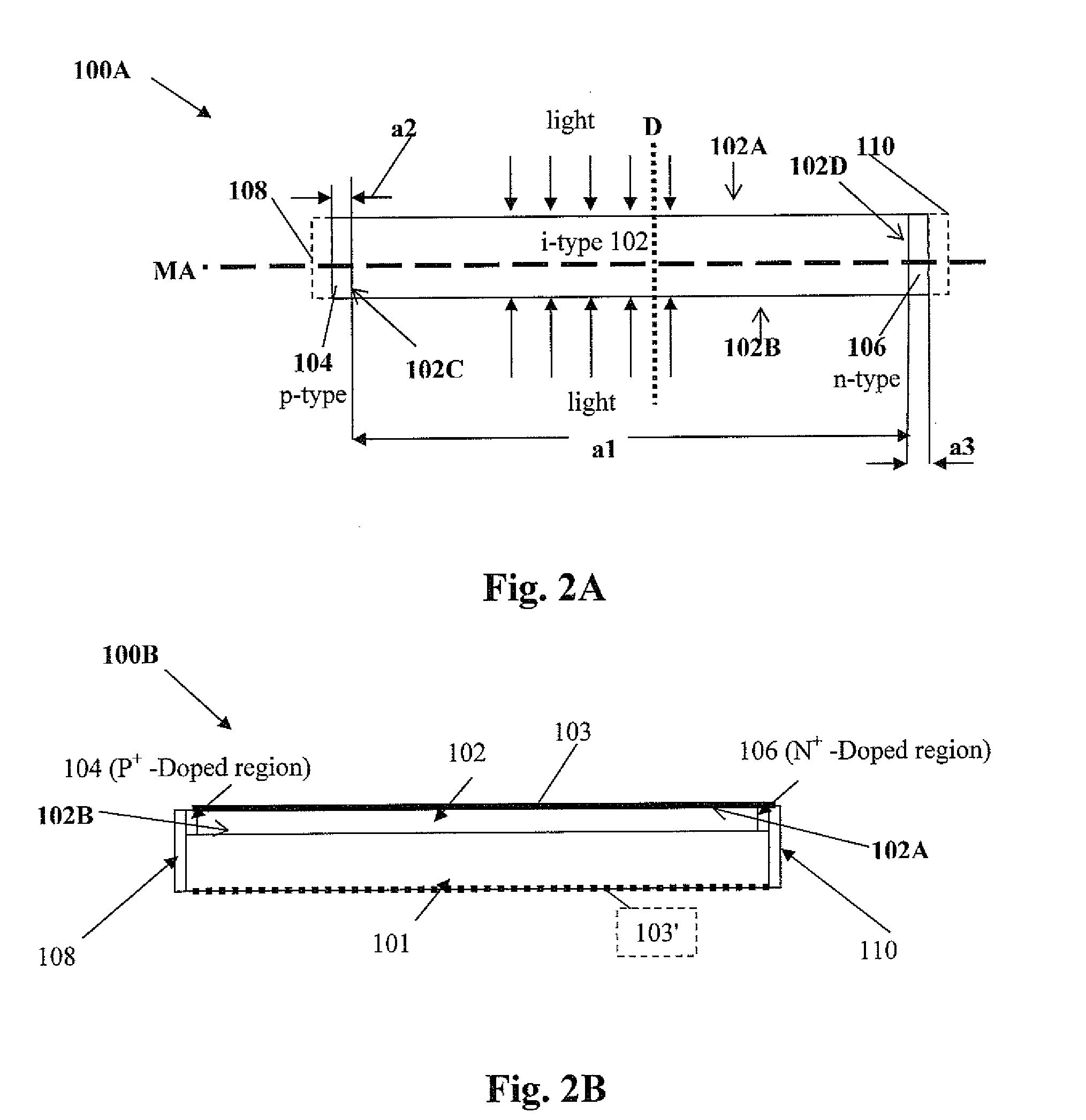
photoelectric conversion efficiency. The present invention solves the above problems by providing a photoelectric structure constructed and operable according on a novel approach. The structure comprises one or more PiN cells, where the PiN cell is configured as a lateral structure (in the meaning of orientation of its active region with respect to a direction of
light propagation and a direction of an internal
electric field). Such PiN cell is formed by an intrinsic (i.e. i-type) (preferably single-crystalline) bulk of semiconductor material which entirely presents an active region of the PiN cell, in which excess charge carriers are created in response to
photon absorbance therein. This novel approach is based on the inventors' understanding that the efficiency of a photoelectric device could be increased by enlarging the depletion region. The conventional approach is bound by the fact that dimensions (specifically the width) of the depletion region are defined by the P-type and N-type
doping concentrations at the emitter and base parts. In the invention, an active region is constituted by a semiconductor intrinsic bulk, and a PiN structure using such active region is configured as a lateral structure.
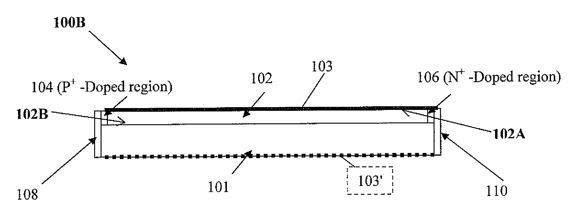
[0019]The PiN cell of the present invention is configured such that, the width dimension of each of the p and n doped regions of the cell is much smaller (practically negligible) relative to that of the active region (
intrinsic semiconductor bulk) in which charge carriers are generated. This provides for increasing the effective active region of the cell of a given lateral dimension thus increasing the efficiency of the cell. However, in order to facilitate collection of the charge carriers, produced in the relatively large active region, a desirably high internal lateral
electric field is created. These conditions are achieved by respectively, appropriate selection of a ratio between the active region size and the doped region size (the minimal value of such ratio is generally of the order of 100, but preferably such ratio is at least about 1000), and selection of appropriate level of
doping of the p- and n-doped regions (concentration of about ˜1019-1021 cm−3—degenerated level of concentration). High
doping concentration in the doped regions, and the low charge carriers concentration in the active region (in the intrinsic region), create high internal electric field (for example of the order of 105 V / cm, e.g. about 1.3*105 V / cm); such internal field is strong enough to sweep the generated excess charge carriers towards the charge carriers collecting region (collecting
electrode associated with the respective doped region). Since the charge carriers move transversally to the photons fall direction (general light incident direction), the photoelectric structure of the present invention is a “lateral” structure, which is contrary to the conventional “vertical” approach.
[0043]It should be noted that the photoelectric structure of the present invention may be used with any
light source whether natural
sunlight or an artificial source and exploits the entire range of the spectrum of the light
radiation.

