Active matrix substrate, method of manufacturing the same, and image sensor incorporating the same

a technology of active matrix substrate and manufacturing method, which is applied in the direction of identification means, radiation controlled devices, instruments, etc., can solve the problems of more signal delays, difficult to tackle tasks through design, aggravating the above problems, etc., and achieve the effect of increasing the number of manufacturing steps and preventing signal transmission delays in signal lines

Inactive Publication Date: 2007-07-31
SHARP KK
View PDF28 Cites 43 Cited by
  • Summary
  • Abstract
  • Description
  • Claims
  • Application Information

AI Technical Summary

Benefits of technology

[0032]In order to solve the foregoing problems, the present invention has an object to offer an active matrix substrate capable of preventing signal transmission delays in signal lines and crosstalk between pixels without an inc

Problems solved by technology

In actual practice, these tasks are hard to tackle by means of designs.
Meanwhile, in medium to small sized display elements, the wires (signal lines 101 and scanning lines 102) inevitably come to have great resistance as the wires are scaled down in breadth to ensure a high aperture ratio with the already narrow pitches remaining unchanged, which results in more signal delays.
The active matrix substrate for use in a sensor needs to clear more strict standards than the active matrix substrate for use in a liquid crystal display device; namely, noise, as well as signal delays, presents a problem that cannot be overlooked.
This is effectively realized by setting the pixel capacitor to a great value; however, that setting would increase the impedance of a pixel capacitor common wire, resulting in aggravation of the aforementioned problems.
The electric potential of the pixel electrode common wire, if oscillates or shifts, can interfere with data, i.e., the electric potentials, for the pixels and thereby cause crosstalk.
Further, if the pixel electrode common wire crosses, and are connected by means of electric capacity to, numerous signal lines, the osc

Method used


Image

  • Active matrix substrate, method of manufacturing the same, and image sensor incorporating the same
  • Active matrix substrate, method of manufacturing the same, and image sensor incorporating the same
  • Active matrix substrate, method of manufacturing the same, and image sensor incorporating the same

Examples


embodiment 1

[0154]Referring to FIG. 1 through FIG. 3, the following description will discuss an embodiment in accordance with the present invention. The manufacturing process of an active matrix substrate shown in FIG. 12(a) through FIG. 12(h) and FIG. 13(a) through FIG. 13(h) is applicable to the active matrix substrate of the present embodiment, and this is one of features of the active matrix substrate of the present embodiment. The following description is made based on these drawings and will focus on differences of the present embodiment from what is illustrated in them. Conventional materials and manufacturing method are applicable to the layers constituting the active matrix substrate of the present embodiment; therefore, description thereof in detail is omitted.

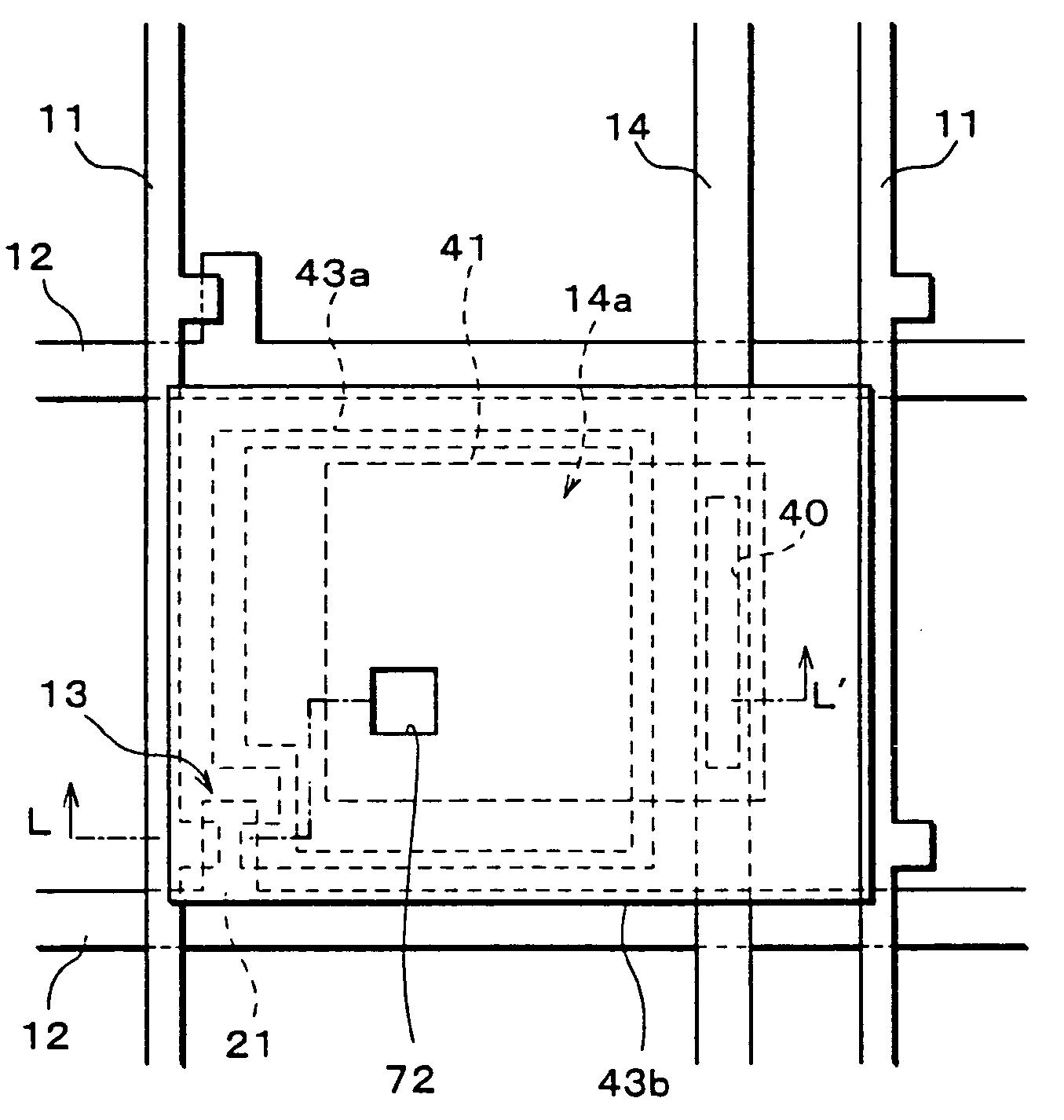
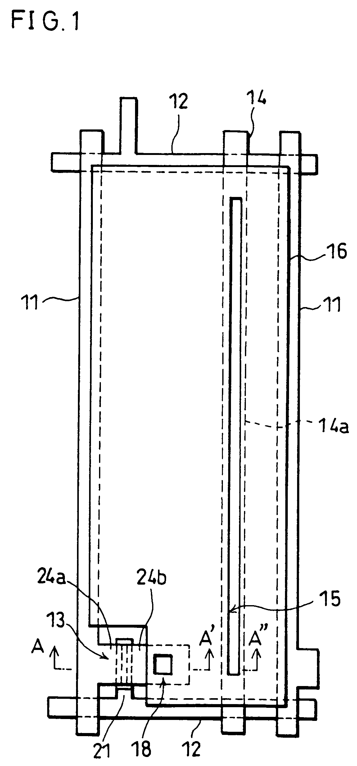
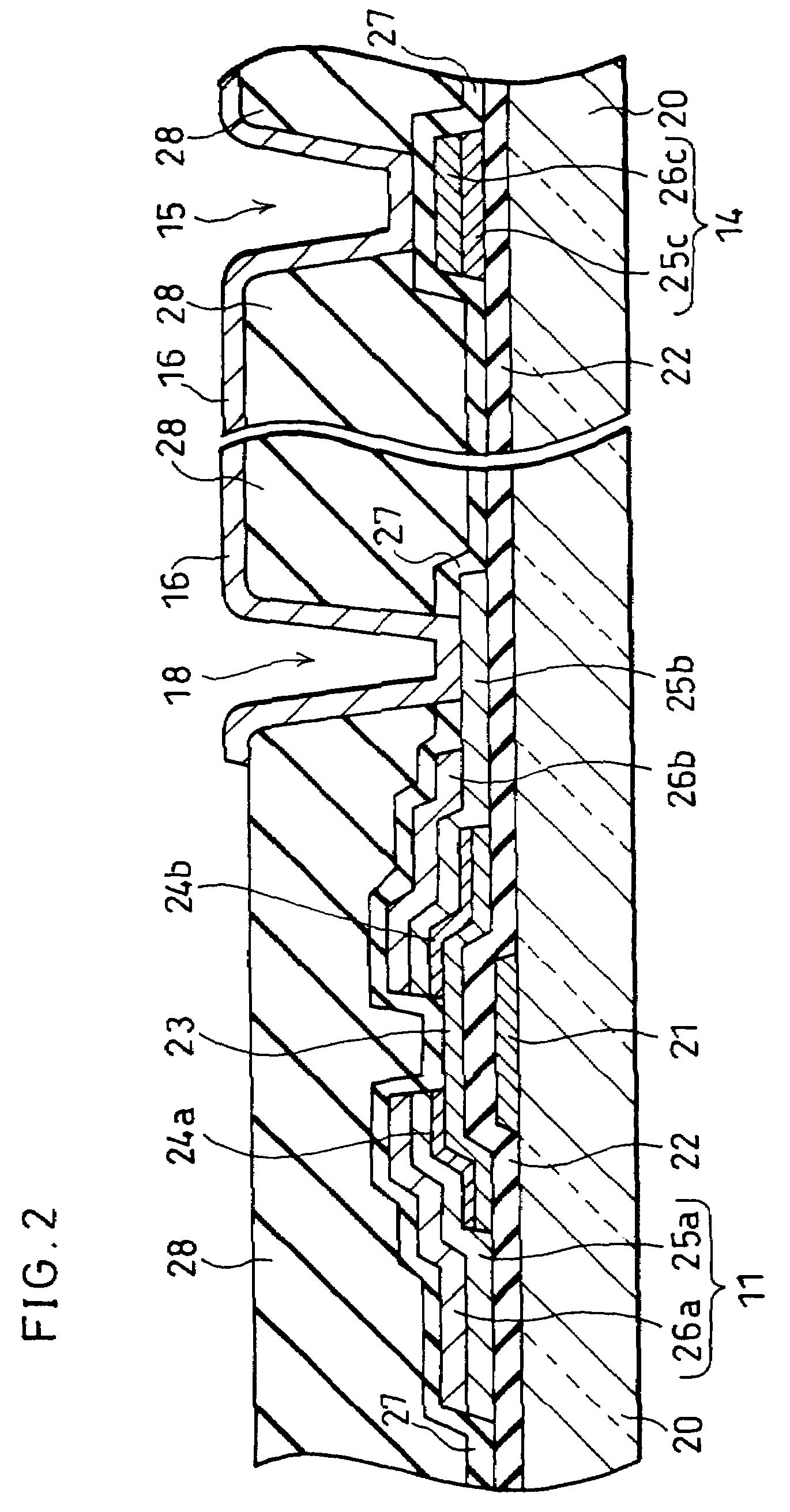
[0155]As shown in FIG. 1 and FIG. 2, the active matrix substrate of the present embodiment includes pixels (pixel area) each encircled by signal lines 11 and scanning lines 12 that are provided in a matrix, and each pixel has a ...

embodiment 2

[0185]Referring to FIG. 4, the following description will discuss another embodiment in accordance with the present invention. Here, for convenience, members of the present embodiment that have the same arrangement and function as members of the first embodiment, and that are mentioned in the first embodiment are indicated by the same reference numerals and description thereof is omitted.

[0186]The active matrix substrate of the present embodiment differs from the active matrix substrate of the first embodiment in the arrangement of pixel capacitor wires. Specifically, in the present embodiment, as shown in FIG. 4, the pixel capacitor wire (storage capacitor common wire) that takes a dual role as a storage capacitor electrode has a single layer structure constituted by a transparent electrode (transparent electrode film) 25c alone. In other words, the patterning of the pixel capacitor wire of the present embodiment is carried out concurrently with the formation of the transparent ele...

embodiment 3

[0191]Chiefly referring to FIG. 5 and FIG. 6, the following description will discuss a further embodiment in accordance with the present invention. Here, for convenience, members of the present embodiment that have the same arrangement and function as members of the previous embodiments, and that are mentioned in the previous embodiments are indicated by the same reference numerals and description thereof is omitted.

[0192]As shown in FIG. 5 and FIG. 6, the active matrix substrate for use in a flat-panel-type x-ray sensor of the present embodiment (hereinafter will be simply referred to as an x-ray sensor) includes pixels each encircled by signal lines 11 and scanning lines 12 that are provided in a matrix, and each pixel has a TFT 13 as a switching element near the point where the signal line 11 crosses the scanning line 12. Each pixel is provided with a transparent electrode (transparent electrode film) 25d as a pixel capacitor wire (storage capacitor common wire), a pixel electrod...


PUM


Abstract

A signal line and a pixel capacitor wire that doubles as a pixel capacitor electrode are fabricated parallel to each other from the same electrode layer through patterning thereof. Therefore, no additional steps are required to form the pixel capacitor wire. In such an arrangement, the pixel capacitor wire and the signal line are disposed parallel to each other; therefore, delays of signal transmission in the signal line and crosstalk between pixels are prevented from occurring. The active matrix substrate incorporating this arrangement is suitably used in liquid crystal display devices, image sensors, and the like. Similar advantages are available with an arrangement in which the signal line and the pixel capacitor wire are disposed parallel to each other, and the storage capacitor electrode, which will constitute a storage capacitor with the pixel electrode therebetween, and the scanning line are fabricated from the same electrode layer through patterning thereof.

Description

[0001]This application is a divisional of application Ser. No. 09 / 520,609, filed Mar. 7, 2000 now U.S. Pat. No. 6,784,949, the entire content of which is hereby incorporated by reference in this application.FIELD OF THE INVENTION[0002]The present invention relates to active matrix substrates for use in, for example, liquid crystal display devices and flat-panel-type image sensors, and methods of manufacturing such substrates, and further relates to image sensors incorporating such active matrix substrates.BACKGROUND OF THE INVENTION[0003]An active matrix substrate for use in, for example, a liquid crystal display device is primarily constituted by electrode wires that are signal lines and scanning lines disposed in a matrix, pixel electrodes each provided for a pixel that is encircled by the signal lines and the scanning lines, and switching elements.[0004]Each of the switching elements, if it is of a double terminal type, is connected to one of the pixel electrodes as well as to ei...

Claims


Application Information

Patent Timeline
IPC IPC(8): G02F1/1343G02F1/136G02F1/1362G02F1/1368G09F9/30H01L21/336H01L27/14H01L27/146H01L29/786H04N1/028H04N5/335H04N5/359H04N5/369H04N5/374
CPCG02F1/136213H01L27/14609H01L27/14
Inventor NAGATA, HISASHIIZUMI, YOSHIHIROSHIMADA, TAKAYUKI
Owner SHARP KK
Why Eureka
Try Eureka