Mounting structure, electro-optical device, electronic apparatus, and method of producing the mounting structure

a technology of mounting structure and mounting plate, which is applied in the direction of semiconductor devices, semiconductor/solid-state device details, instruments, etc., can solve the problems of difficult balance between the electrical connection between the bump electrode and the counter electrode, the non-uniform or large contact resistance or contact defects of the mounting portion, and the adhesion between the bump and the base layer, so as to reduce the manufacturing time and cost of the electronic component, increase the number of manufacturing steps, and the effect of not increasing the number of manufacturing

Inactive Publication Date: 2008-05-01
EPSON IMAGING DEVICES CORP
View PDF7 Cites 4 Cited by
  • Summary
  • Abstract
  • Description
  • Claims
  • Application Information

AI Technical Summary

Benefits of technology

[0022]In the manufacturing method, although the base regions may be directly formed on the bump during the formation of the base layer, the base regions are formed in such a manner that the base layer is partly processed with such gas or liquid passing through the microstructures as described above. Therefore, it is not necessary to precisely control conditions for forming the base layer. This allows the base regions to be readily formed.
[0023]In the manufacturing method, it is preferable that the conductive surface layer be formed and then patterned. Furthermore, the following operations are simultaneously performed: an operation of partly processing the base layer to form the base regions and an operation of patterning the base layer using the patterned conductive surface layer as a mask. This prevents an increase in the number of manufacturing steps, resulting in a reduction in the manufacturing time and cost of the electronic component. That is, since an operation of forming only the base regions is not necessary, the number of manufacturing steps is not increased and the manufacturing time and cost of the electronic component can be reduced.
[0024]In the manufacturing method, it is preferable that the bump be treated so as to have a rough surface in the forming operation of the bump, the base layer have surface irregularities which are due to the rough surface of the bump and which are formed in the forming operation of the base layer, and the microstructures be formed in the forming operation of the conductive surface layer in such a manner that the conductive surface layer is provided on the surface irregularities of the base layer. This allows the base layer to be tightly bonded to the bump and also allows the microstructures to be readily formed.

Problems solved by technology

However, the bump electrode has a problem that a mounting portion has non-uniform or large contact resistance or contact defects.
This is because the first conductive sublayer has ductility lower than that of the second conductive sublayer and therefore cracks when the bump electrode is distorted during mounting, which can cause cracks in the second conductive sublayer.
In general, it is difficult to balance the electrical connection between the bump electrode and a counter electrode and the adhesion between the bump and the base layer.

Method used


Image

  • Mounting structure, electro-optical device, electronic apparatus, and method of producing the mounting structure
  • Mounting structure, electro-optical device, electronic apparatus, and method of producing the mounting structure
  • Mounting structure, electro-optical device, electronic apparatus, and method of producing the mounting structure

Examples


Embodiment Construction

[0039]Configuration of Electronic Component (Semiconductor Device)

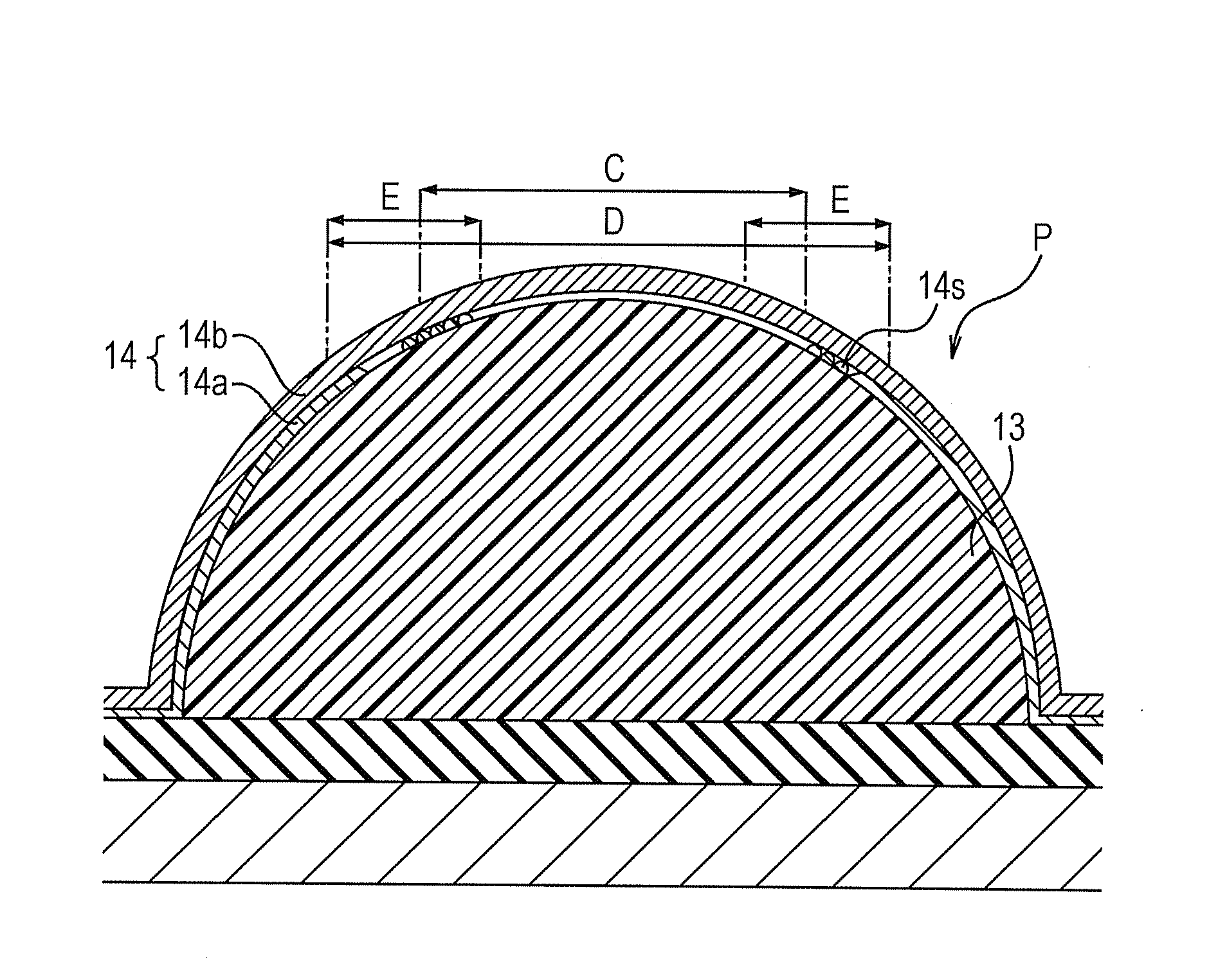
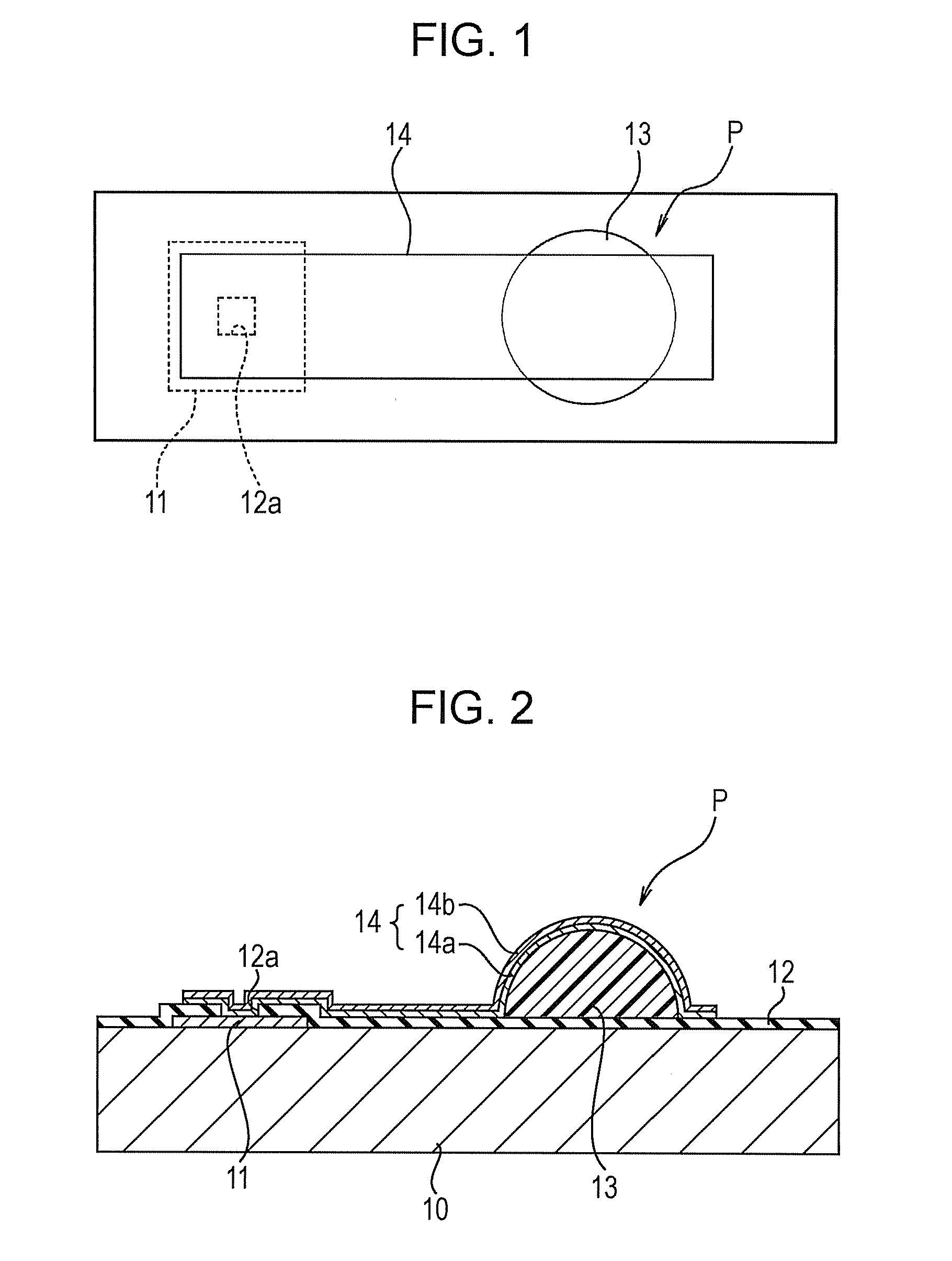
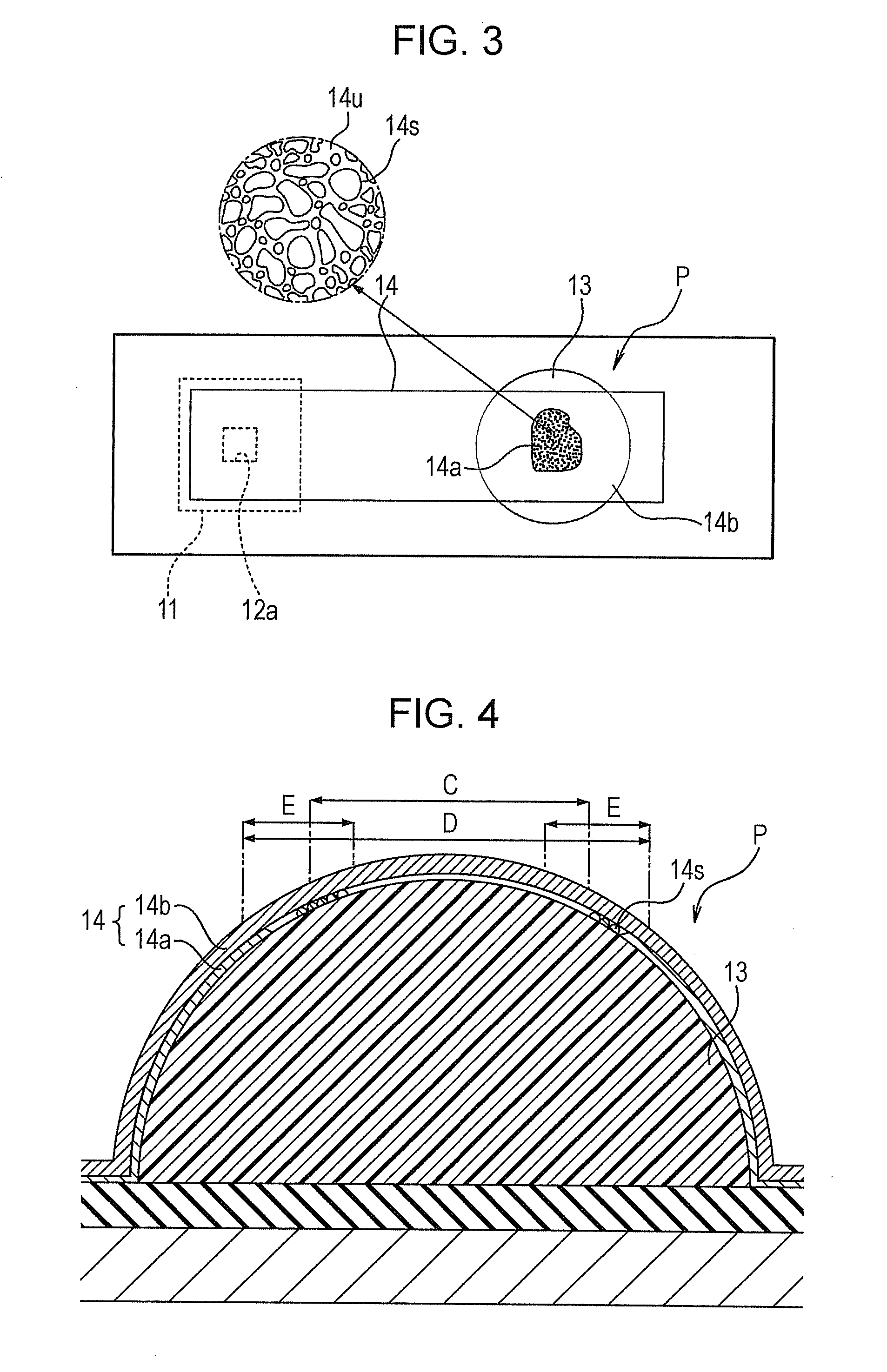
[0040]Embodiments of the present invention will now be described in detail with reference to the accompanying drawings. FIG. 1 is a fragmentary plan view of an electronic component or semiconductor device according to an embodiment of the present invention. FIG. 2 is a fragmentary vertical sectional view of the electronic component or the semiconductor device. In this embodiment, a base electrode 11 made of aluminum (Al) or the like is disposed on a substrate 10, such as a semiconductor substrate, made of single-crystalline silicon. An insulating layer 12, made of silicon dioxide (SiO2) or silicon nitride (SiN), having an opening 12a extends over the substrate 10 and the base electrode 11. The base electrode 11 has a portion exposed from the opening 12a. A bump electrode P is disposed on the insulating layer 12. The bump electrode P includes a bump 13 and a conductive layer 14 as described below in detail.

[0041]The bu...


PUM


Abstract

A semiconductor device includes a bump electrode including a bump made of resin, a base layer disposed on the bump, and a conductive surface layer disposed on the base layer. The base layer has ductility lower than that of the conductive surface layer and includes base regions which are spaced from each other and which are arranged at least in a top zone of the bump electrode.

Description

[0001]The entire disclosure of Japanese Patent Application No. 2006-289580, filed Oct. 25, 2006 is expressly incorporated by reference herein.BACKGROUND[0002]1. Technical Field[0003]The present invention relates to a semiconductor device, a mounting structure, an electro-optical apparatus, an electronic system, and a method for manufacturing an electronic component including a bump electrode.[0004]2. Related Art[0005]In general, electronic components for semiconductor devices include substrates and bump electrodes disposed thereon. The bump electrodes are attached to mounting boards such that electronic components are electrically connected to the mounting boards. Examples of the bump electrodes include metal bump electrodes that are prepared in such a manner that a thick coating of a metal such as gold (Au) is deposited on each seed electrode portion. Examples of a mounting technique using the bump electrodes include techniques for mounting driving integrated circuits on substrates...

Claims


Application Information

Patent Timeline
Patent Type & Authority Applications(United States)
IPC IPC(8): H01L23/48H01L21/44
CPCG02F1/13452H01L24/11H01L2924/0001H01L2224/13684H01L2224/13671H01L2224/13664H01L2224/13655H01L2224/13647H01L2224/1319H01L2224/13666H01L2924/01033H01L2924/01024H01L2924/01023H01L2924/01006H01L24/13H01L2224/1358H01L2924/14H01L2924/01079H01L2924/01078H01L2924/01074H01L2924/01049H01L2924/01047H01L2924/01046H01L2924/01029H01L2224/13099H01L2924/01013H01L2924/01015H01L2924/01022H01L2924/0665H01L2924/00014H01L2224/13008H01L2224/05022H01L2224/05548H01L2224/05001H01L2224/05124H01L2224/05147H01L2224/05155H01L2224/05164H01L2224/05166H01L2224/05171H01L2224/05184H01L2224/05639H01L2224/05644H01L2224/05647H01L2224/05669H01L2224/0235H01L2224/02313H01L24/02H01L2924/013
Inventor SAITO, ATSUSHI
Owner EPSON IMAGING DEVICES CORP
Why Eureka
Try Eureka