Semiconductor memory device provided with a write column selection switch and a read column selection switch separately

a memory device and switch technology, applied in the field of semiconductor memory devices, can solve the problems of difficult optimization of column selection timing, and achieve the effect of extending the time required by through-current to flow

Inactive Publication Date: 2007-07-31
HITACHI LTD
View PDF15 Cites 3 Cited by
  • Summary
  • Abstract
  • Description
  • Claims
  • Application Information

AI Technical Summary

Benefits of technology

[0009]An object of the present invention is to provide a technical means to reduce a through-current.
[0010]Another object of the present invention is to provide a technical means to easily optimize the column selection timing.
[0014]According to the means described above, the column selection switch for write and the column selection switch for read are operated in different timings and thereby reduction of through-current may be attained. In more practical, since the Y selection line WYS for write to control the operation of the column selection switch in the write amplifier is isolated from the Y selection line RYS for read to control the operation of the column selection switch in the read amplifier, the column selection switch in the read amplifier may be set to the non-operating condition during the write operation. As a result, a through-current during the write operation may be reduced.
[0015]Moreover, since the write IO line and read IO line are allocated crossing the sense amplifier column and the column selection line for write and column selection line for read are allocated in parallel to the sense amplifier column, the wiring area of the column selection lines can be attained. In more practical, when the Y selection line YS is isolated to the Y selection line WYS for write and the Y selection line RYS for read, the total number of Y selection lines is increased up to two times in comparison with the total number when the Y selection line YS is not isolated. Therefore, the write IO line and read IO line are allocated crossing the sense amplifier column, and the column selection line for write and column selection line for read are allocated in parallel to the sense amplifier column in order to employ the layout where the small number of Y selection lines YS are used. Accordingly, even when the total number of Y selection lines YS is doubled, the wiring area of the Y selection lines YS may be acquired easily.
[0018]Moreover, when a semiconductor memory device is comprised of a lead IO line to read the data, a main amplifier to read and amplify the data of IO line and a precharge circuit to precharge the read IO line, it is also possible to provide a means to start the precharge of the read IO line with the precharge circuit in the timing that the operation of main amplifier is started. This means may be realized, in more practical, with a main amplifier control circuit. Here, to realize the high-speed read operation, it is required to quickly assert the IO precharge control signal for read in order to realize quick precharge of IO line for read. However, when the timing to start the precharge is set quickly, the time required by the through-current to flow may be so far extended. Therefore, increase of the through-current when the precharge timing is set quickly may be avoided by quickly setting the Y selection line for read to the non-selecting condition. Such control may be realized easily by fetching the main amplifier control signal outputted from the main amplifier control circuit as the decoding condition of the decoder. The same effect can also be attained even when the timing to assert the IO precharge control signal for read is set almost equal to the timing to set the Y selection line for read to the non-selecting condition.

Problems solved by technology

However, in the circuit structure to control the operations of the column selection switch for write which can transfer the write data transferred via the write IO line to the bit line and the column selection switch for read which can selectively transfer the read data of bit line to the read IO line with the common control signal, since it is impossible to independently control the column selection switch for write and the column selection switch for read, it is assumed difficult to optimize the column selection timing.
In addition, even in the circuit structure to independently control the column switch for read and the column switch for write with the signal lines, it is still difficult to optimize the column selection timing, if it is not obvious how the control signal is generated and then supplied.

Method used


Image

  • Semiconductor memory device provided with a write column selection switch and a read column selection switch separately
  • Semiconductor memory device provided with a write column selection switch and a read column selection switch separately
  • Semiconductor memory device provided with a write column selection switch and a read column selection switch separately

Examples


Embodiment Construction

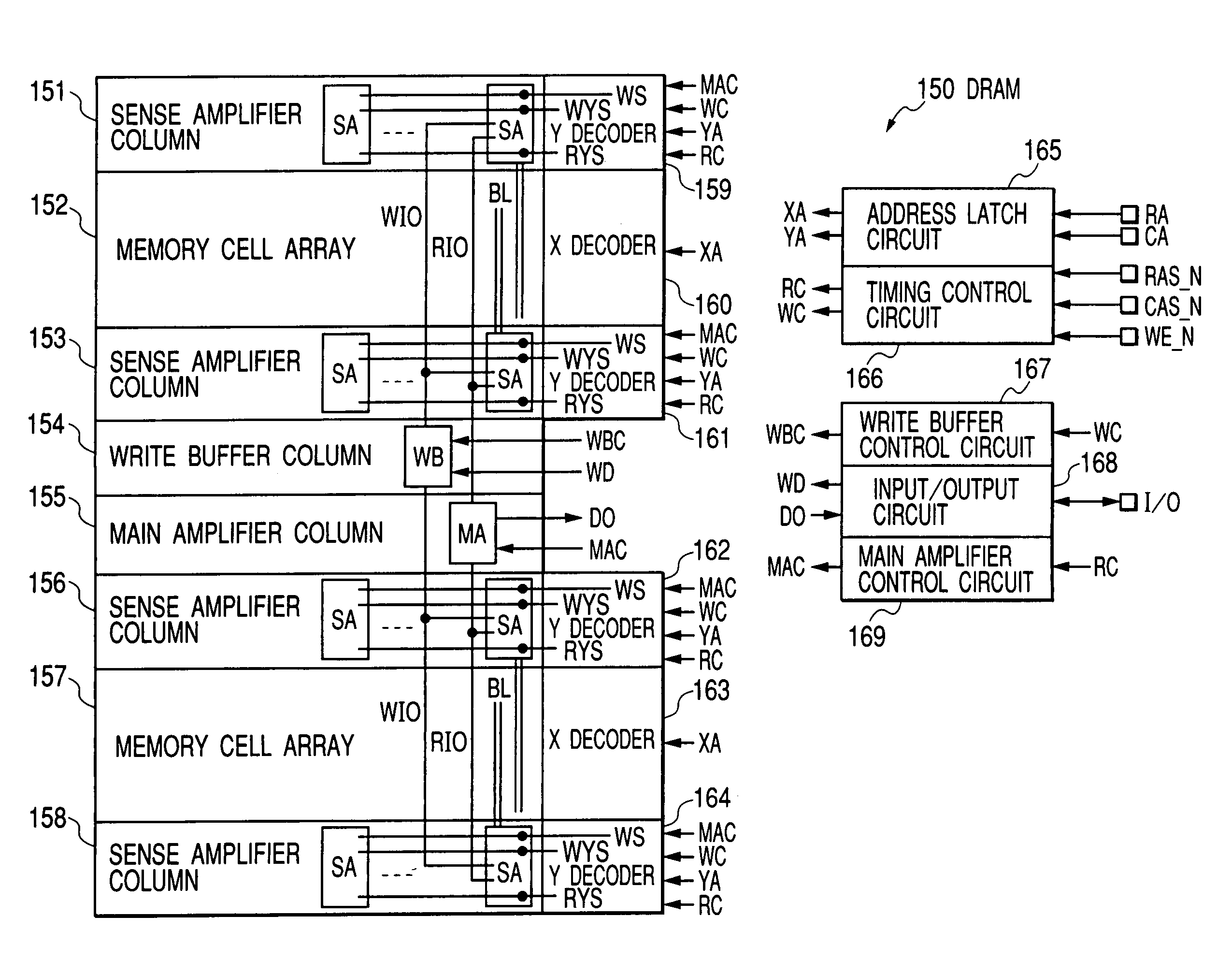
[0034]FIG. 15 illustrates a DRAM (Dynamic Random Access Memory) which is an example of a semiconductor memory device of the present invention.

[0035]The DRAM 150 illustrated in FIG. 15 comprises, although not particularly restricted, sense amplifier columns 151, 153, 156, 158, memory cell arrays 152, 157, a main amplifier column 155, a write buffer column 154, Y (column) decoders 159, 161, 162, 164, X (row) decoders 160, 163, an address latch circuit 165, a timing control circuit 166, a write buffer control circuit 167, an input / output circuit 168, and a main amplifier control circuit 169 and is then formed on one semiconductor substrate such as a single crystal silicon substrate with the well known semiconductor integrated circuit manufacturing technique.

[0036]The memory cell arrays 152, 157 are formed of a matrix layout of a plurality of dynamic memory cells. The selection terminal of this memory cell is connected to the word line in each row direction, while the data input termina...


PUM


Abstract

A Y selection line for write for controlling operations of a column selection switch within a write amplifier and a Y selection line for read for controlling operations of a column selection switch within a read amplifier are provided individually and the column selection switch within the read amplifier is set to the non-operating condition during the write operation. Accordingly, a through-current during the write operation may be reduced. In this case, the write IO line and read IO line are allocated crossing sense amplifier columns, while the column selection line for write and column selection line for read are allocated in parallel to the sense amplifier columns.

Description

CROSS-REFERENCE TO RELATED APPLICATION[0001]This application is a Continuation application of U.S. application Ser. No. 10 / 625,573 filed Jul. 24, 2003 now abandoned. Priority is claimed based on U.S. application Ser. No. 10 / 625,573 filed Jul. 24, 2003, which claims the priority of Japanese Patent Application No. 2002-218020 filed Jul. 26, 2002, all of which is incorporated by reference.BACKGROUND OF THE INVENTION[0002]The present invention relates to a semiconductor memory device and more particularly to a technical means to reduce a through-current flowing in the same device and a technical means to optimize the column selection timing.[0003]As an example of a semiconductor memory device, a dynamic random access memory (hereinafter, abbreviated as “DRAM”) has been proposed. This DRAM is comprised of a plurality of dynamic memory cells which are allocated in the structure of an array. Regarding such semiconductor memory device, a technical means has been proposed to utilize a column...

Claims


Application Information

Patent Timeline
Patent Type & Authority Patents(United States)
IPC IPC(8): G11C5/06A01K29/00G11C5/00H01L27/108G11C7/10G11C11/401G11C11/407G11C11/4076H01L21/8242
CPCG11C7/1078G11C7/1096G11C11/4076G11C2207/002G11C2207/229
Inventor SAKAMOTO, MASATOSHIHASEGAWA, MASATOSHI
Owner HITACHI LTD
Why Eureka
Try Eureka