Piezo-TFT cantilever MEMS

a thin film transistor and cantilever technology, applied in the direction of fluid pressure measurement, acceleration measurement using interia forces, instruments, etc., can solve the problems of difficult and expensive standardization, varied mems structure, and limited crystallization procedures,

Inactive Publication Date: 2007-08-07
SHARP KK
View PDF3 Cites 57 Cited by
  • Summary
  • Abstract
  • Description
  • Claims
  • Application Information

AI Technical Summary

Problems solved by technology

The crystallization procedures are also limited by the temperature sensitivity of the substrate material.
MEMS structures are varied and, therefore, more difficult to standardize, as compared to the above-mentioned thin film processes.
Many of the MEMS devices that have been fabricated to date have more theoretical than practical application, as the devices are often difficult and expensive to make.
For the same reason, larger scale systems using MEMS components, have been expensive to fabricate due to the process difficulties and the cost associated with integrating the MEMS and IC technologies.
However, the etching processes needed to form a bulk silicon MEMS are more difficult to control, dramatically limit available process steps, and require long etch times. These limitations make these devices unsuitable for low-cost integrated systems.
However, these sensing schemes cannot be applied to low temperature TFT process, because the changes in electrical characteristics induced as a result of stress change are too small to be practically measured.

Method used


Image

  • Piezo-TFT cantilever MEMS
  • Piezo-TFT cantilever MEMS
  • Piezo-TFT cantilever MEMS

Examples


Embodiment Construction

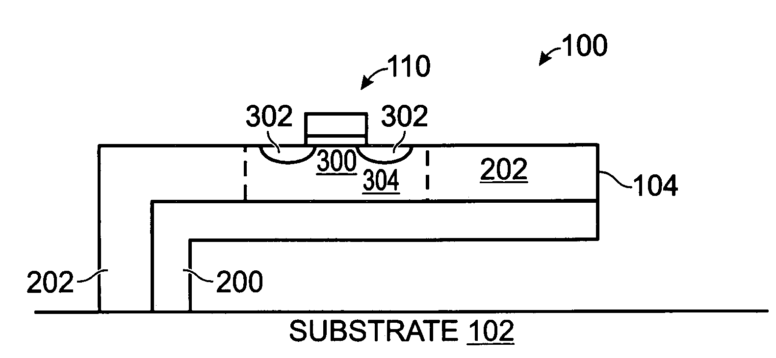
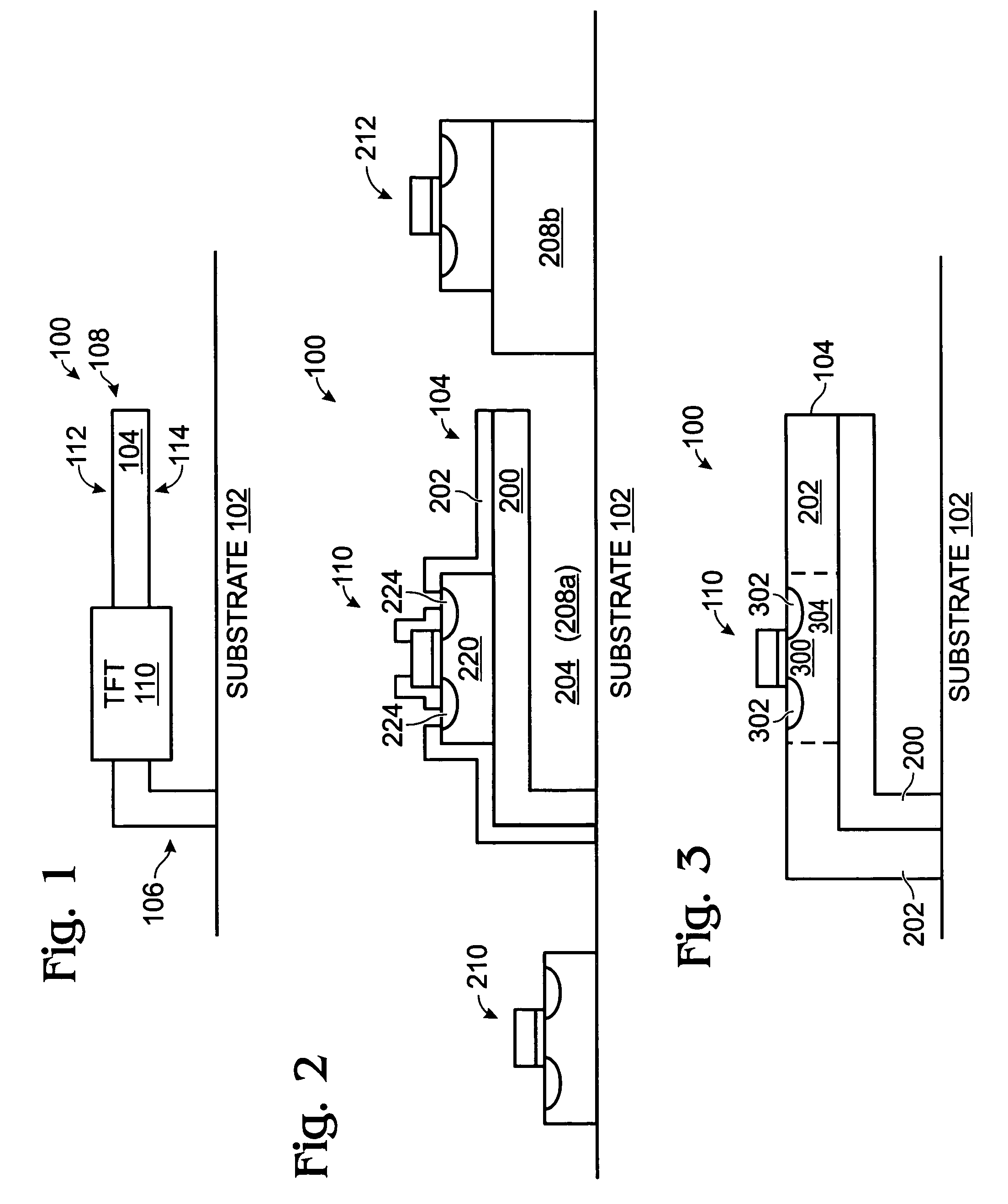
[0040]FIG. 1 is a partial cross-sectional view of a piezo thin-film transistor (piezo-TFT) cantilever microelectromechanical system (MEMS). The piezo-TFT cantilever 100 comprises a substrate 102, made from a material such as glass, polymer, quartz, metal foil, Si, sapphire, ceramic, or compound semiconductor materials. A thin-film cantilever beam 104 has a distal end 106, anchored to the substrate 102, and a proximal end 108. Note, in other aspects not shown both the distal end and the proximal end can be anchored to substrate. Also, the shape of the cantilever body can be a simple beam shape, any membrane shape, or combinations of beam shapes and membrane shapes, with one or multiple anchors to the substrate. A TFT 110 is shown within the cantilever beam 104. The cantilever beam 104 and TFT 110 are made from materials such as a-Si, poly-Si, oxides, a-SiGe, poly-SiGe, metals, metal-containing compounds, nitrides, polymers, ceramic films, magnetic films, or compound semiconductor mat...


PUM


Abstract

A piezo-TFT cantilever microelectromechanical system (MEMS) and associated fabrication processes are provided. The method comprises: providing a substrate, such as glass for example; forming thin-films overlying the substrate; forming a thin-film cantilever beam; and simultaneously forming a TFT within the cantilever beam. The TFT is can be formed least partially overlying a cantilever beam top surface, at least partially overlying a cantilever beam bottom surface, or embedded within the cantilever beam. In one example, forming thin-films on the substrate includes: selectively forming a first layer with a first stress level; selectively forming a first active Si region overlying the first layer; and selectively forming a second layer overlying the first layer with a second stress level. The thin-film cantilever beam is formed from the first and second layers, while the TFT source / drain (S / D) and channel regions are formed from the first active Si region.

Description

RELATED APPLICATIONS[0001]This application is a continuation-in-part of a pending patent application entitled, CRYSTAL-STRUCTURE-PROCESSED MECHANICAL DEVICES AND METHODS AND SYSTEMS FOR MAKING, invented by John Hartzell, Ser. No. 10 / 131,318, filed Apr. 23, 2002.[0002]This application is a continuation-in-part of a pending patent application entitled, THIN-FILM CRYSTAL-STRUCTURE-PROCESSED DEVICES AND METHODS AND SYSTEMS FOR MAKING, invented by John Hartzell, Ser. No. 10 / 131,006, filed Apr. 23, 2002.[0003]This application is a continuation-in-part of a patent application entitled, SEMICONDUCTOR CRYSTAL-STRUCTURE-PROCESSED MECHANICAL, AND METHODS AND SYSTEMS FOR MAKING, invented by John Hartzell, Ser. No. 10 / 131,057, filed Apr. 23, 2002, now U.S. Pat. No. 6,860,939.[0004]This application is a continuation-in-part of a pending patent application entitled, MONOLITHIC INTEGRATED CRYSTAL-STRUCTURE-PROCESSED MECHANICAL, AND COMBINED MECHANICAL AND ELECTRICAL DEVICES, AND METHODS AND SYSTEMS...

Claims


Application Information

Patent Timeline
Patent Type & Authority Patents(United States)
IPC IPC(8): H01L27/14H01L21/336
CPCB81B3/0021B81C1/00246C30B1/02G01L1/044G01L9/0042G01P15/0802G01P15/124C30B29/00B81B2201/0292B81B2203/0118B81C2203/075H01L27/12H01L29/66757H04R17/02H04R31/006G01P2015/0828
Inventor ZHAN, CHANGQINGWOLFSON, MICHAEL BARRETTHARTZELL, JOHN W.
Owner SHARP KK
Why Eureka
Try Eureka