Automatic mercury probe for use with a semiconductor wafer

a technology of mercury probes and semiconductor wafers, applied in electrical testing, measurement devices, instruments, etc., can solve problems such as unrepeatable probe measurements to an ultra-shallow layer

Inactive Publication Date: 2007-08-07
FOUR DIMENSIONS
View PDF4 Cites 14 Cited by
  • Summary
  • Abstract
  • Description
  • Claims
  • Application Information

AI Technical Summary

Benefits of technology

[0017]The initial refreshing of the mercury before each probing ensures clean, good mercury contacts for each automatic probing, as well as contributing to the containment of the mercury to prevent unclean mercury (e.g., oxidized or debris containing mercury) being advanced to the next position of the test wafer, or a new test wafer, where it may stick to the surface of the wafer rather than only contacting

Problems solved by technology

Uniform probing contact of the wafer results in less current concentration at the point of test current injection, and soft probing minimizes crystal deformation which causes the energy

Method used


Image

  • Automatic mercury probe for use with a semiconductor wafer
  • Automatic mercury probe for use with a semiconductor wafer
  • Automatic mercury probe for use with a semiconductor wafer

Examples


Embodiment Construction

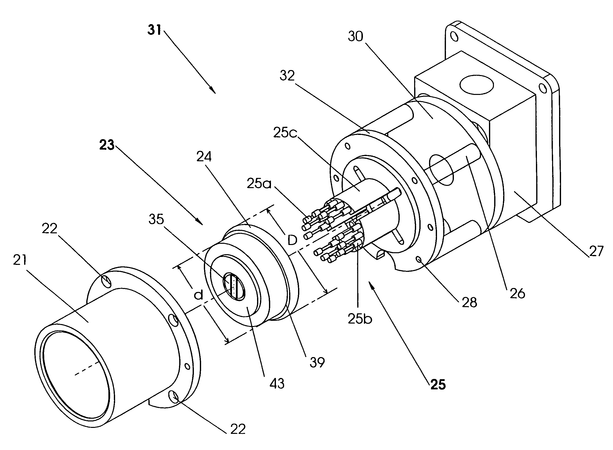
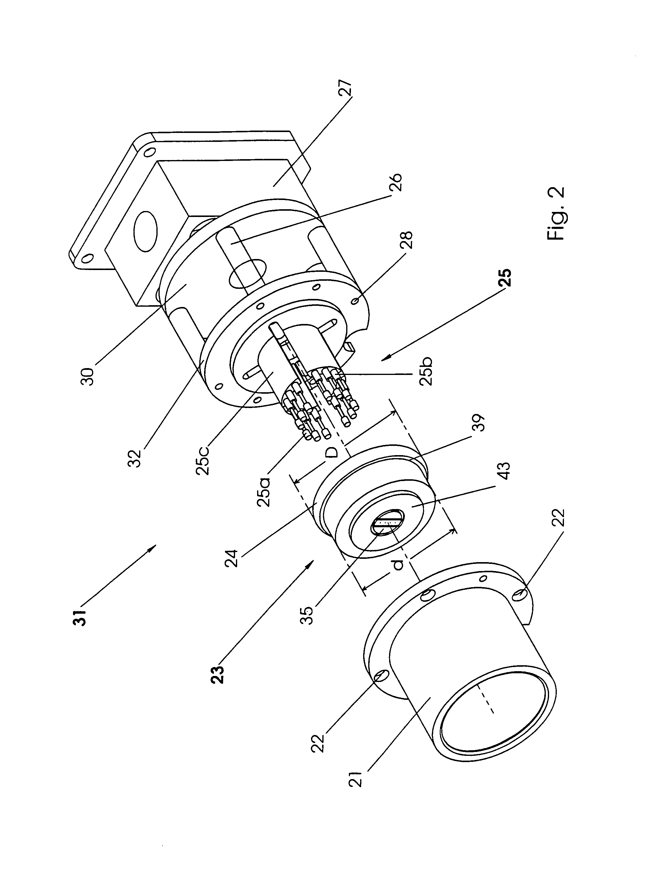
[0034]As will be seen from the following discussion, the multi-point probe of the present invention, illustrated in the following discussion as a four-point probe, utilizes mercury, which is electrically conductive, drawn up through four small diameter tubes and passages in a probe head by means of a vacuum as mercury probes for testing a semiconductor wafer. Additionally, it will become clear to one skilled in the art that an extremely small diameter mercury contact provides a small diameter electrically conductive probe of the surface of the wafer to minimizing probe penetration of the wafer, mechanically and electrically, in order to minimize disturbance to the ultra-shallow implanted layer on the wafer for more accurate sheet resistivity measurements.

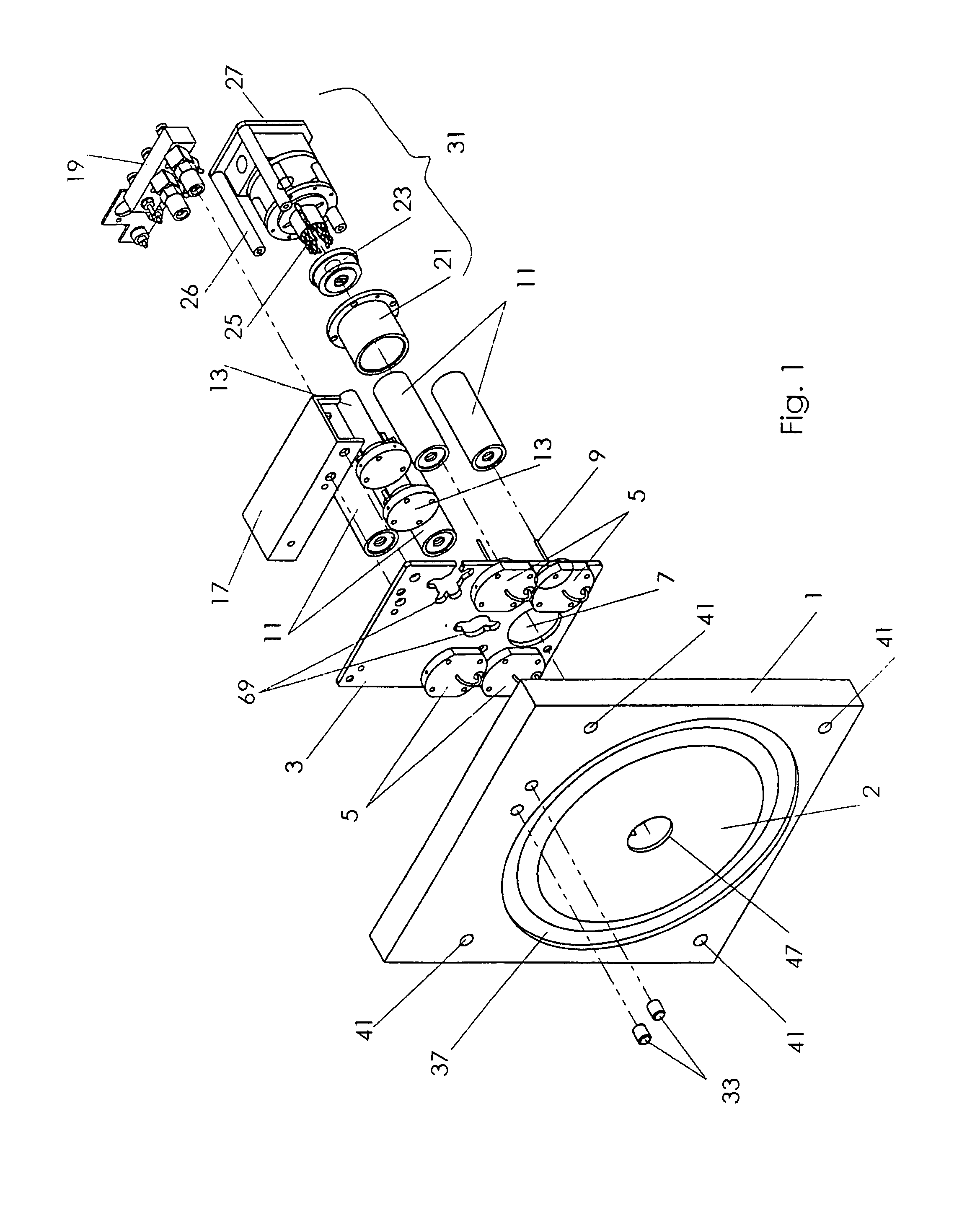
[0035]FIG. 1 is an exploded perspective view of the mercury four-point probe system of the present invention minus electrical cabling, and vacuum components and tubing. This has been done to make the mechanical structure of the pres...


PUM


Abstract

An upward facing probing mechanism using mercury probe contacts for accurate automatic multi-site measurements of a semiconductor wafer, especially of ultra-shallow ion implanted layers on a semiconductor wafer held top surface facing downward. A fixed force is applied to the wafer regardless of the thickness of the wafer through the of use of a regulated pressure piston. Incorporated are a plurality of spring-loaded rod assemblies to support the floating probe head to position the probe head face into full contact with the wafer surface accurately placing all mercury contacts on the surface of the wafer regardless of the inclination of the wafer as a result of the even support of the probe head by the spring-loaded rod assemblies. Included is a mechanism to refresh the mercury contacts for each probing with full containment and recovery of the mercury used in each probing.

Description

CROSS-REFERENCE[0001]This patent application claims priority from an application by the same title having Ser. No. 10 / 912,422 filed Aug. 4, 2004 now abandoned with that application claiming priority from a Provisional Patent Application having Ser. No. 60 / 493,870 that was filed on Aug. 7, 2003.BACKGROUND OF THE INVENTION[0002]1. Field of the Invention[0003]This invention relates to probe system for use with semiconductor wafers. More particularly, it relates to a probe system having an upward facing probe head disposed to interface with the top surface of a wafer-under-test with the wafer held upside down by a wafer support chuck. Said probe system including an evenly spring-supported, gas piston push-pulled, upward-facing probe head, wherein one or more mercury electrodes of various shape and area can be formed to make low-pressure uniform and clean contacts in the upward facing orientation with the upside down held wafer-under-test. Said probe head, being evenly spring-supported, ...

Claims


Application Information

Patent Timeline
IPC IPC(8): G01R31/02
CPCG01R1/06783G01R31/2891
Inventor CHEN, JAMES T.
Owner FOUR DIMENSIONS
Why Eureka
Try Eureka