

High performance spin-valve transistor
a high-performance, spin-valve technology, applied in the field of spin-valve transistors, can solve the problems of limiting the intensity of the emitter current isub>e/sub>, difficult to produce and difficult to achieve significant schottky junction level differences
- Summary
- Abstract
- Description
- Claims
- Application Information
AI Technical Summary
Benefits of technology
Problems solved by technology
Method used
Image

Examples
Embodiment Construction
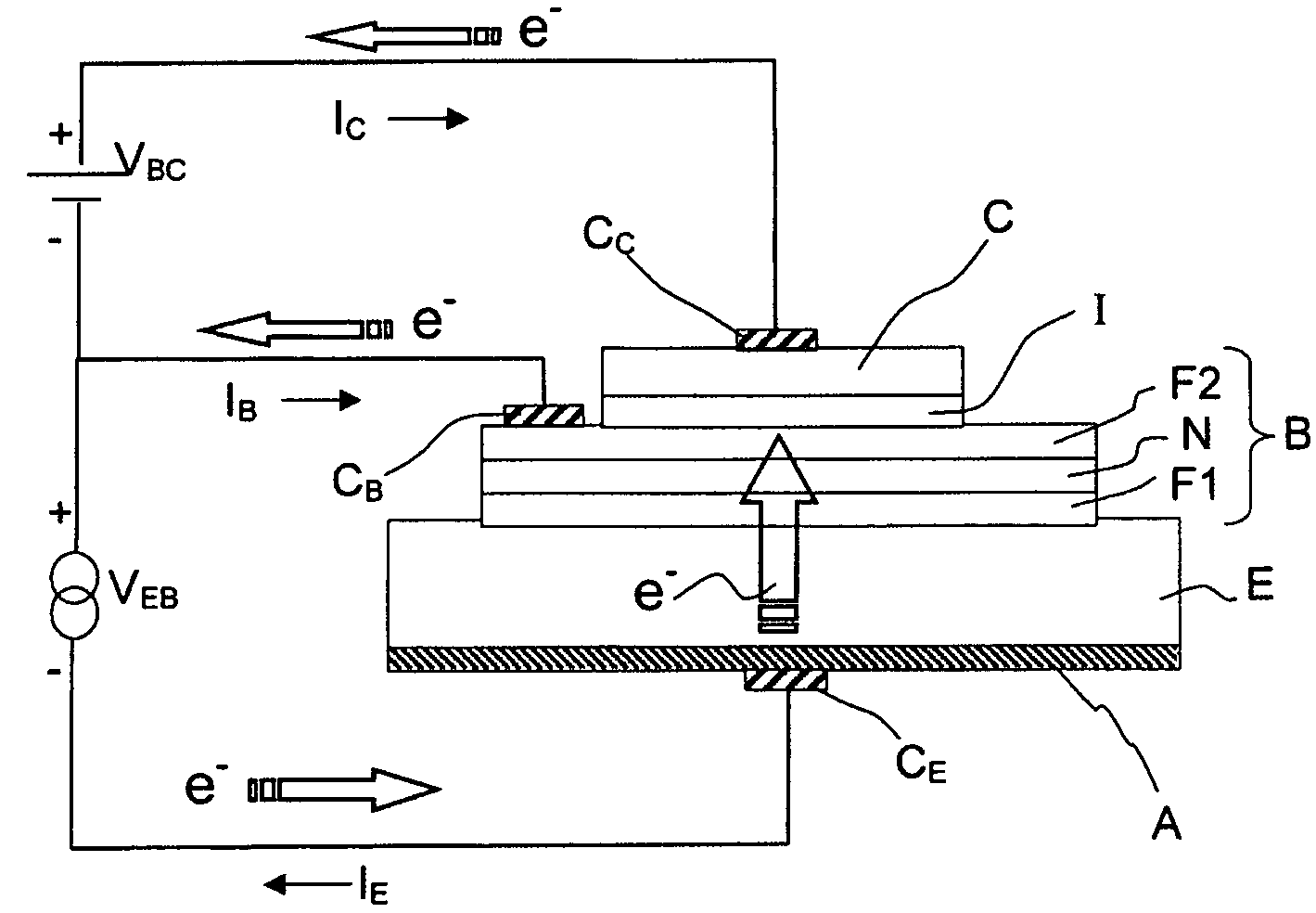
[0038]FIG. 5 represents a symbolic diagram of the spin-valve transistor according to the invention. It comprises an emitter E of semiconductor material, a metallic base B made up of three layers F1, N and F2 forming a spin valve, an insulating material I and a collector C of electrically conductive material. The emitter / base junction is of Schottky type as indicated in FIG. 5. The arrow indicates the direction of the collected current. Electrons are injected from the emitter to the base through the emitter / base Schottky junction. The electrons pass from the base B to the collector C through the insulator I either by tunnel effect or ballistically. This arrangement has two major advantages over the prior arrangements. The use of a Schottky type emitter / base junction allows higher emitter / base voltages VEB to be used, no longer limited by the breakdown phenomenon. It is thus possible to obtain high emitter currents IE and, consequently, high collector currents IC. Since the base is fo...
PUM
 Abstract
Description
Claims
Application Information