
Methods of reducing power in programmable logic devices using low voltage swing for routing signals

a programmable logic and routing signal technology, applied in the direction of power consumption reduction, logic circuits using specific components, pulse techniques, etc., can solve the problems of high leakage current, high leakage current, and difficulty in minimizing leakage current, so as to reduce the internal signaling power consumption of a programmable logic devi

Inactive Publication Date: 2007-08-28
ALTERA CORP
View PDF5 Cites 1 Cited by
  • Summary
  • Abstract
  • Description
  • Claims
  • Application Information

AI Technical Summary

Benefits of technology

The present invention provides better ways to reduce the power consumption of a programmable logic device. This is done by reducing the amount of charge that needs to be routed through the device's resources. The invention includes driver circuitry that limits the routing signal from being driven all the way to the device's power supply. This results in a more efficient device that consumes less power.

Problems solved by technology

With the current trend in scaling down device geometries (e.g., 0.18 μm process down to 0.13 μm, 90 nm, 65 nm, or lower) and the consequent use of ever-lower operating voltages (e.g., supply voltages, bias voltages, etc.), which are nearing levels comparable to VT, the ability of transistor pass gate structures to function at relatively high speeds while at the same time minimizing leakage current is a difficult design hurdle to overcome.
Moreover, this trend of smaller device geometries and consequent use of lower operating voltages is creating a design tradeoff between speed (e.g., response time for the pass gate transistor to turn ON) and leakage current (e.g., the current that passes through the pass gate transistor when turned OFF) that was not previously experienced with larger device geometries and the consequent use of higher operating voltages.
That is, if conventional design techniques are applied to smaller device geometries, high speed pass gate operation is accompanied with high leakage current, whereas low leakage current is accompanied with low speed pass gate operation.
High leakage current is undesirable because it results in excess heat, power loss, and poorer performance.
Another problem associated with shrinking geometries is the consequent use of lower operating voltages.
This lower operating voltage is typically a nominal voltage supplied to the device, and may be insufficient for certain circuitry, such as configurable memory cells (e.g., SRAM) within the device, to operate properly.
A large percentage of a device's power is consumed by the capacitive charging and discharging of the interconnection conductors.
This can lead to several problems in conventional PLD interconnection circuitry.
For example, signaling slows down and the circuitry becomes increasingly susceptible to capacitive cross-talk between parallel conductors.

Method used


Image

  • Methods of reducing power in programmable logic devices using low voltage swing for routing signals
  • Methods of reducing power in programmable logic devices using low voltage swing for routing signals
  • Methods of reducing power in programmable logic devices using low voltage swing for routing signals

Examples


Embodiment Construction

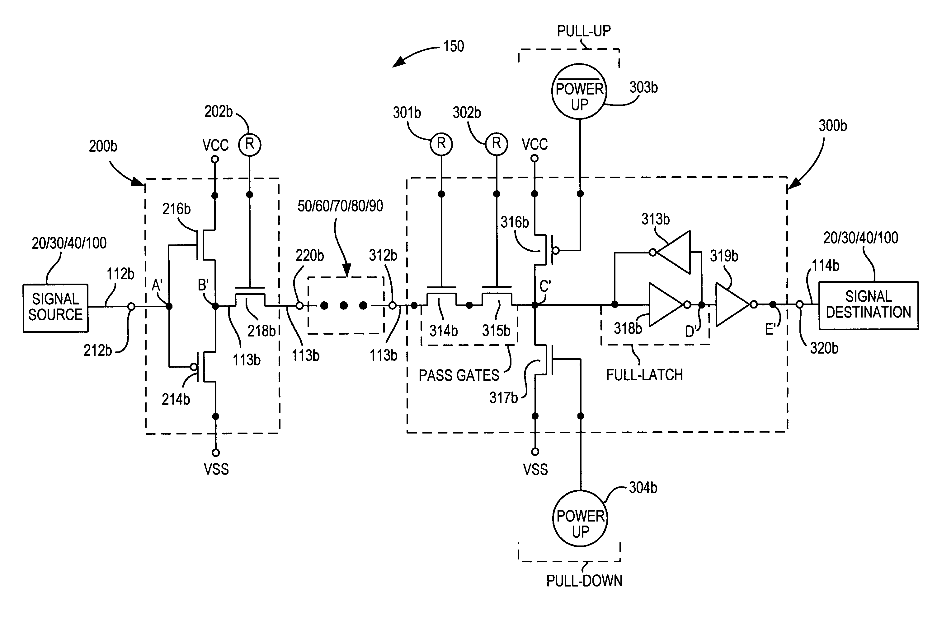
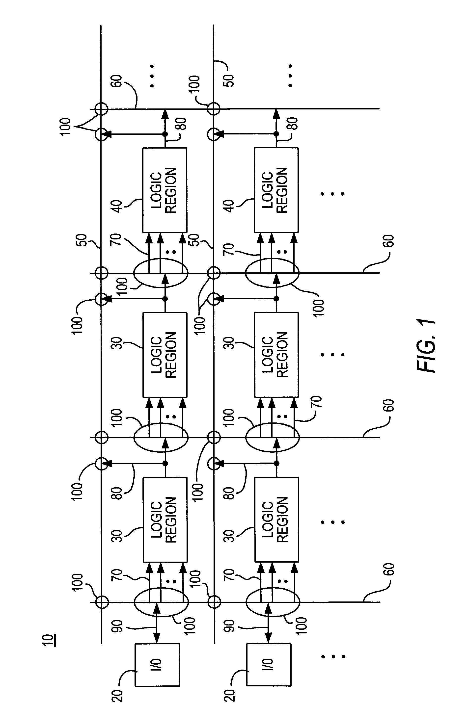
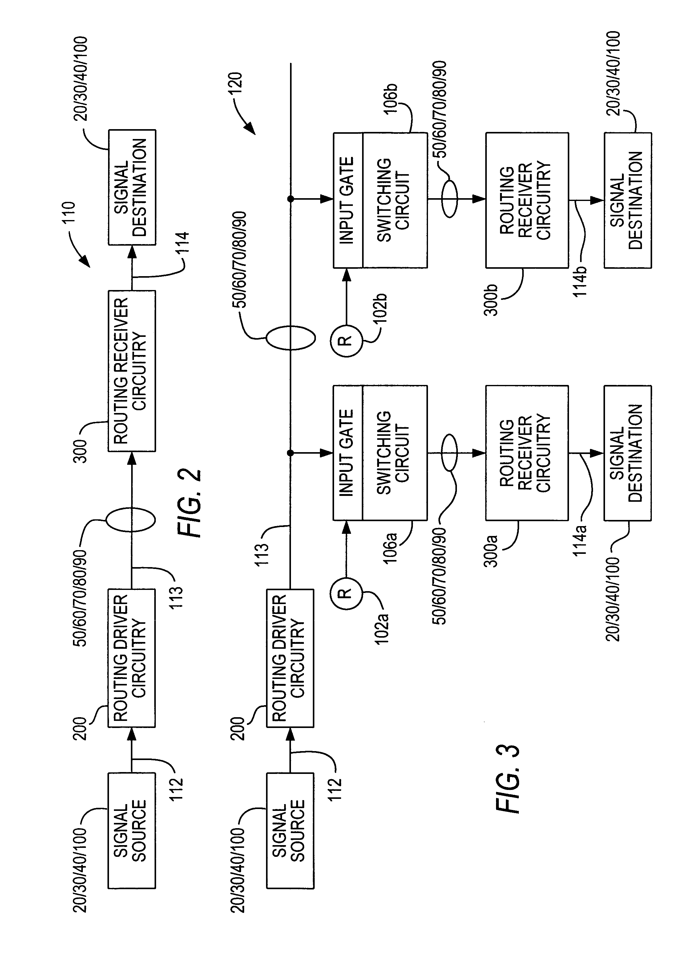
[0024]FIG. 1 shows a representative portion of an illustrative PLD 10 that can be constructed in accordance with the invention. PLD 10 includes regions 20 of input / output (I / O) circuitry, regions 30 of programmable logic, and regions 40 of user-accessible memory. Other types of operational circuitry (e.g., microprocessor circuitry) may also be included on PLD 10. For example, such other circuitry may be in addition to what is shown in FIG. 1, or it may take the place of some of regions 40. Interconnection resources are also included on PLD 10. These resources include horizontal interconnection resources 50, vertical interconnection resources 60, region feeding resources 70, region output resources 80, and I / O serving resources 90. (Single lines in FIG. 1 may represent multiple, substantially parallel conductors.) The interconnection resources also include programmable connections between the various types of other interconnection resources. These programmable connections are represe...


PUM


Abstract

Reduced voltage swing signal path circuitry is provided that lowers the internal signaling power consumption of the interconnection resources of a programmable logic device. The reduced voltage swing signal path circuitry includes a reversed routing driver circuitry to limit the voltage range of the output signal of the driver circuitry.

Description

BACKGROUND OF THE INVENTION[0001]The present invention relates generally to programmable logic devices (PLDs), and more particularly to reducing power consumption in such devices.[0002]It should be noted that the term PLD as used herein is intended to cover the broad space of programmable logic. This includes devices commonly known as CPLDs (Complex Programmable Logic Devices) such as MAX 7000® from Altera Corporation of San Jose, Calif., FPGAs (Field Programmable Gate Arrays) such as Stratix® from Altera, or Structured ASICs (metal programmable logic) such as Hardcopy® from Altera.[0003]Examples of known programmable logic devices are shown in Cliff et al. U.S. Pat. Nos. 5,909,126 and 5,963,049, which are hereby incorporated by reference herein in their entireties. PLDs typically include large numbers of regions of programmable logic and other operational resources such as memory, input / output circuits, etc., that are selectively interconnectable via programmable interconnection re...

Claims


Application Information

Patent Timeline
Patent Type & Authority Patents(United States)
IPC IPC(8): H03K19/177
CPCH03K19/0013H03K19/17736H03K19/17784
Inventor LANE, CHRISTOPHERSANTURKAR, VIKRAM
Owner ALTERA CORP
Learn More