

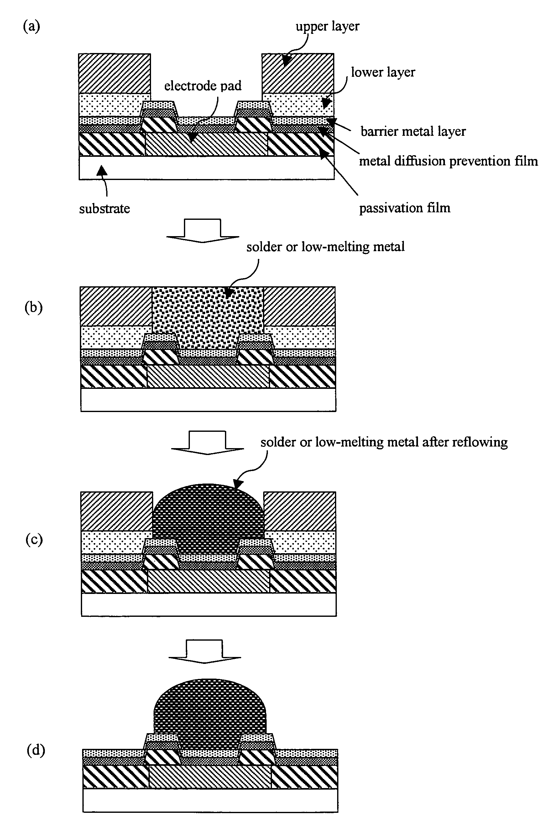
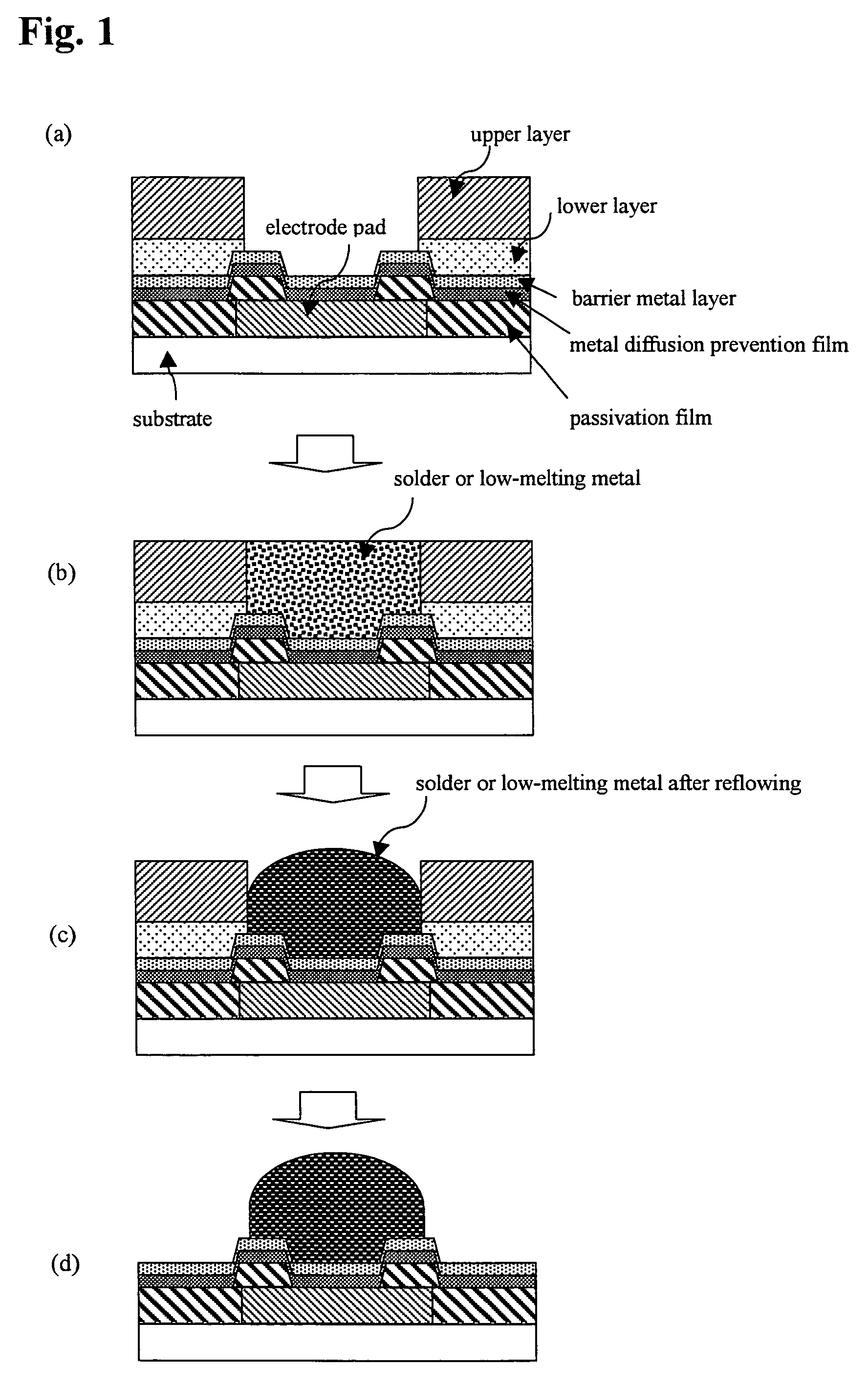
Method for forming bump on electrode pad with use of double-layered film
a technology of double-layer film and bump, which is applied in the field of lowmelting metal bump forming process, can solve the problems of non-uniform bump size, resist becomes even more difficult to peel from the board, and is generally difficult to peel, so as to inhibit curing reaction, good peelability of laminated two-layer film, and poor peelability
- Summary
- Abstract
- Description
- Claims
- Application Information
AI Technical Summary
Benefits of technology
Problems solved by technology
Method used
Image

Examples
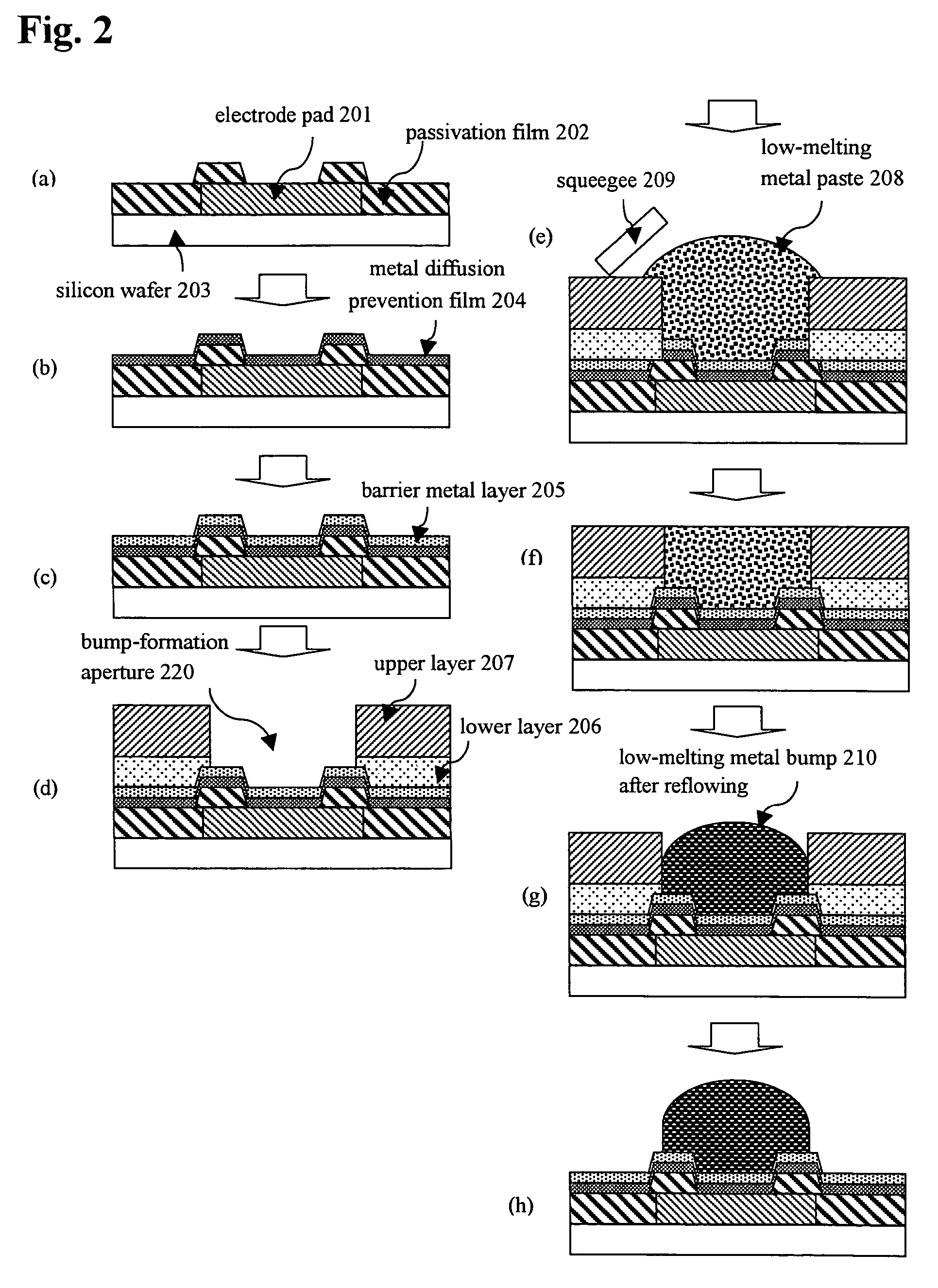
example 1
[0157]The lower layer material A-L was spin coated over the evaluation board A, and the coating was baked on a hot plate at 120° C. for 5 minutes to give a lower layer 5 μm thick. On the lower layer, the upper layer material A-L was spin coated, and the coating was baked on a hot plate at 120° C. for 5 minutes to give an upper layer having a thickness of 65 μm.
[0158]The laminated film was photoexposed through a patterned glass mask with ultraviolet rays from a high-pressure mercury lamp with use of an aligner (MA-150, available from Suss Microtech Inc.) in a manner such that the dose was 1000 mJ / cm2 at a wavelength of 420 nm. During the photoexposure, the glass mask was brought into intimate contact with the board covered with the PET film.
[0159]The above-photoexposed board was subjected to paddle development in an aqueous solution containing 2.38% tetramethylammoniumhydroxide (hereinafter, abbreviated as TMAH developing solution). The developer application time was generally 90 sec...
example 2
[0176]The lower layer material A-L was spin coated over the evaluation board A, and the coating was baked on a hot plate at 120° C. for 5 minutes to give a lower layer 5 μm thick. On the lower layer, the upper layer material A-D (thickness: 65 μm) was laminated.
[0177]The other procedures were carried out in the same manner as in Example 1.
example 3
[0178]The lower layer material B-L was spin coated over the evaluation board B, and the coating was baked in a clean oven at 110° C. for 10 minutes to give a lower layer 2 μm thick. On the lower layer, the upper layer material B-L was spin coated, and the coating was baked at 110° C. for 10 minutes to give an upper layer having a thickness of 40 μm.
[0179]The laminated film was photoexposed through a patterned glass mask with ultraviolet rays from a high-pressure mercury lamp with use of an aligner (MA-150, available from Suss Microtech Inc.) in a manner such that the dose was 400 mJ / cm2 at a wavelength of 350 nm. During the photoexposure, the glass mask was brought into intimate contact with the board covered with the PET film.
[0180]In the photoexposure, the hole pattern (first aperture pattern) of the evaluation board was aligned with a second aperture pattern of the radiation-sensitive resin composition.
[0181]The above-photoexposed board was subjected to development by being showe...
PUM
| Property | Measurement | Unit |
|---|---|---|
| thickness | aaaaa | aaaaa |
| thickness | aaaaa | aaaaa |
| thickness | aaaaa | aaaaa |
Abstract
Description
Claims
Application Information