Memory device for controlling nonvolatile and volatile memories

a memory device and nonvolatile technology, applied in the direction of memory adressing/allocation/relocation, instruments, digital storage, etc., can solve the problems of low data reliability, disadvantageous or flash memory b>902/b>, error of actual data in the buffer b>1001/b>, etc., to achieve high speed

Inactive Publication Date: 2007-09-04
VALLEY DEVICE MANAGEMENT
View PDF16 Cites 28 Cited by
  • Summary
  • Abstract
  • Description
  • Claims
  • Application Information

AI Technical Summary

Benefits of technology

[0028]It is still another object of the present invention to provide a memory device capable of correcting and writing spare data in a NAND flash memory at a high speed.

Problems solved by technology

However, the NOR flash memory 902 is disadvantageous because of its small capacity, large size, and high power consumption.
However, the NAND flash memory 905 can only be sequentially accessed and therefore requires the RAM 906 to enable a random access.
Although the NAND flash memory 905 has the above advantages, it requires the error detection and correction circuit 903 because data reliability is low.
When the two data are not the same, it means that the actual data in the buffer 1001 has an error.
For this reason, the number of processing steps is large, and the processing speed is low.
This means that the data transfer requires a long time.
For this reason, the microcontroller 901 can not use its original low power supply voltage, and so low power consumption cannot be realized.

Method used


Image

  • Memory device for controlling nonvolatile and volatile memories
  • Memory device for controlling nonvolatile and volatile memories
  • Memory device for controlling nonvolatile and volatile memories

Examples


Embodiment Construction

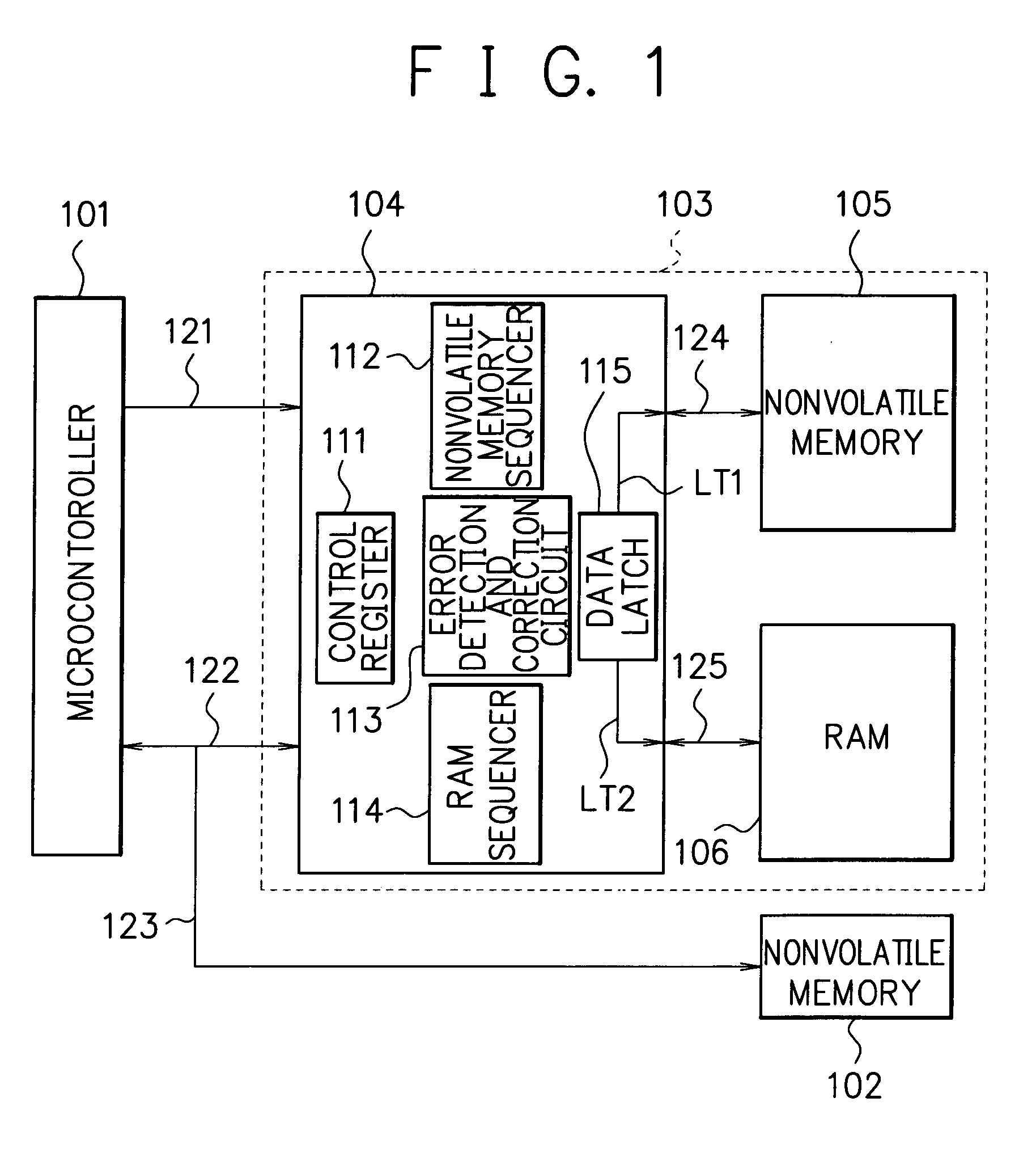
[0044]FIG. 1 is a block diagram showing the construction of a memory device according to an embodiment of the present invention.

[0045]A microcontroller 101 is connected to an internal controller 104 through external buses 121 and 122. The external bus 121 is a controller control signal line, and the external bus 122 is a RAM interface line 122.

[0046]The internal controller 104 is connected to a nonvolatile memory (NV memory) 105 through a memory bus 124 and to a RAM 106 through a memory bus 125. The nonvolatile memory 105 is, e.g., a NAND flash memory. The RAM 106 is, e.g., an SRAM (Static Random Access Memory). The memory bus 124 is a NAND flash memory interface bus. The memory bus 125 is a RAM interface bus. The internal controller 104, the NAND flash memory 105, and the RAM 106 are incorporated in a single package 103.

[0047]The internal controller 104 includes a control register 111, a NAND flash memory sequencer 112, an error detection and correction circuit 113, a RAM sequencer...


PUM


Abstract

A memory device includes a nonvolatile memory capable of storing data, a volatile memory capable of being random-accessed, and a controller for transferring data between the nonvolatile memory and the volatile memory and enabling a pseudo access as if the volatile memory were externally directly accessed in accordance with an instruction through an external bus when the data transfer is not performed.

Description

CROSS-REFERENCE TO RELATED APPLICATIONS[0001]This application is based upon and claims priority of Japanese Patent Application Nos. JP2001-055104, filed on Feb. 28, 2001 and JP2002-004150, filed on Jan. 11, 2002, the contents being incorporated herein by reference.BACKGROUND OF THE INVENTION[0002]1. Field of the Invention[0003]The present invention relates to memory devices, in particular, including nonvolatile and volatile memories.[0004]2. Description of the Related Art[0005]FIG. 9 is a block diagram showing the construction of a conventional memory device. A microcontroller 901 is connected to a nonvolatile memory (NV memory) 905 through a bus and to a RAM 906, an error correction circuit 903, and a nonvolatile memory 902 through another bus. The nonvolatile memory 902 is a NOR flash memory, and the nonvolatile memory 905 is a NAND flash memory.[0006]The NOR flash memory 902 can be random-accessed. For this reason, the microcontroller 901 can directly access the NOR flash memory ...

Claims


Application Information

Patent Timeline
Patent Type & Authority Patents(United States)
IPC IPC(8): G06F12/00G06F12/16G06F12/06G06F13/16G11C11/00
CPCG06F13/1673G06F13/1684G11C11/005
Inventor HIGUCHI, YOSHINOBUMIZUTANI, SHINJIKANAZAWA, KEISUKE
Owner VALLEY DEVICE MANAGEMENT
Why Eureka
Try Eureka