Power management for circuits with inactive state data save and restore scan chain

a technology of power management and scan chain, applied in the field of integrated circuit devices, can solve the problems of inability to prevent power loss by leakage current, loss of all information held in a circuit, and inability to secure a storage area

Inactive Publication Date: 2007-09-11
SOCIONEXT INC
View PDF21 Cites 69 Cited by
  • Summary
  • Abstract
  • Description
  • Claims
  • Application Information

AI Technical Summary

Benefits of technology

[0014]An integrated circuit device according to an aspect of the present invention is an integrated circuit device comprising at least one functional module which outputs save data in synchronism with a saving clock signal, a power supply control unit which selects one of the functional modules, and controls stop and resumption of power supply to the selected functional modu

Problems solved by technology

However, even when the operation of a functional module is stopped by stopping the clock, power is kept supplied to the functional module itself, so power loss by leakage current cannot be prevented.
When the power supply is shut down, all information held in a circuit is lost.
Therefore, it is of course unnecessary to secure a storage area for data saving.
This makes the circuit layout very complicated.
This undesirably increases the number of gates.
However, this method is not preferable b

Method used


Image

  • Power management for circuits with inactive state data save and restore scan chain
  • Power management for circuits with inactive state data save and restore scan chain
  • Power management for circuits with inactive state data save and restore scan chain

Examples


first embodiment

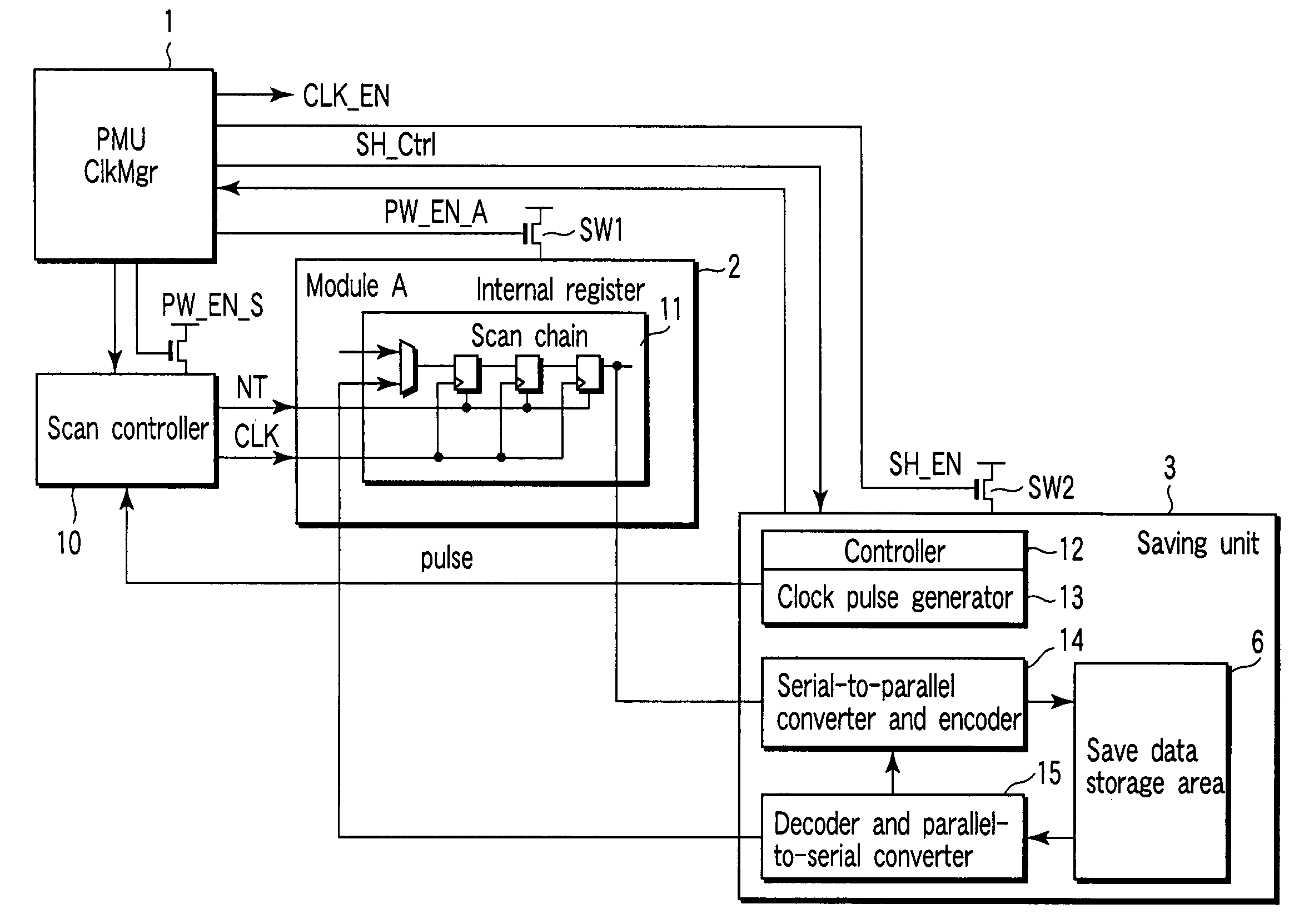
[0054]FIG. 5 is a block diagram showing the first embodiment of the integrated circuit device according to the present invention. The first embodiment is a more practical arrangement of the configuration shown in FIG. 1. As in the configuration shown in FIG. 1, a PMU 1 is the main component for managing power supply control and control of a saving process itself. The PMU 1 is usually installed in an integrated circuit device (LSI) aiming at low power consumption. The PMU 1 controls clock supply and power supply to functional modules 2, thereby minimizing the power consumption in a functional module 2 in an idling state. The PMU 1 can be implemented by software such as an OS (Operating System) or hardware. In either case, the PMU 1 controls clock supply and power supply to a specific functional module on the basis of the process history and waiting time in the integrated circuit device.

[0055]A plurality of functional modules 2 are managed by the PMU 1. The PMU 1 can select any functi...

second embodiment

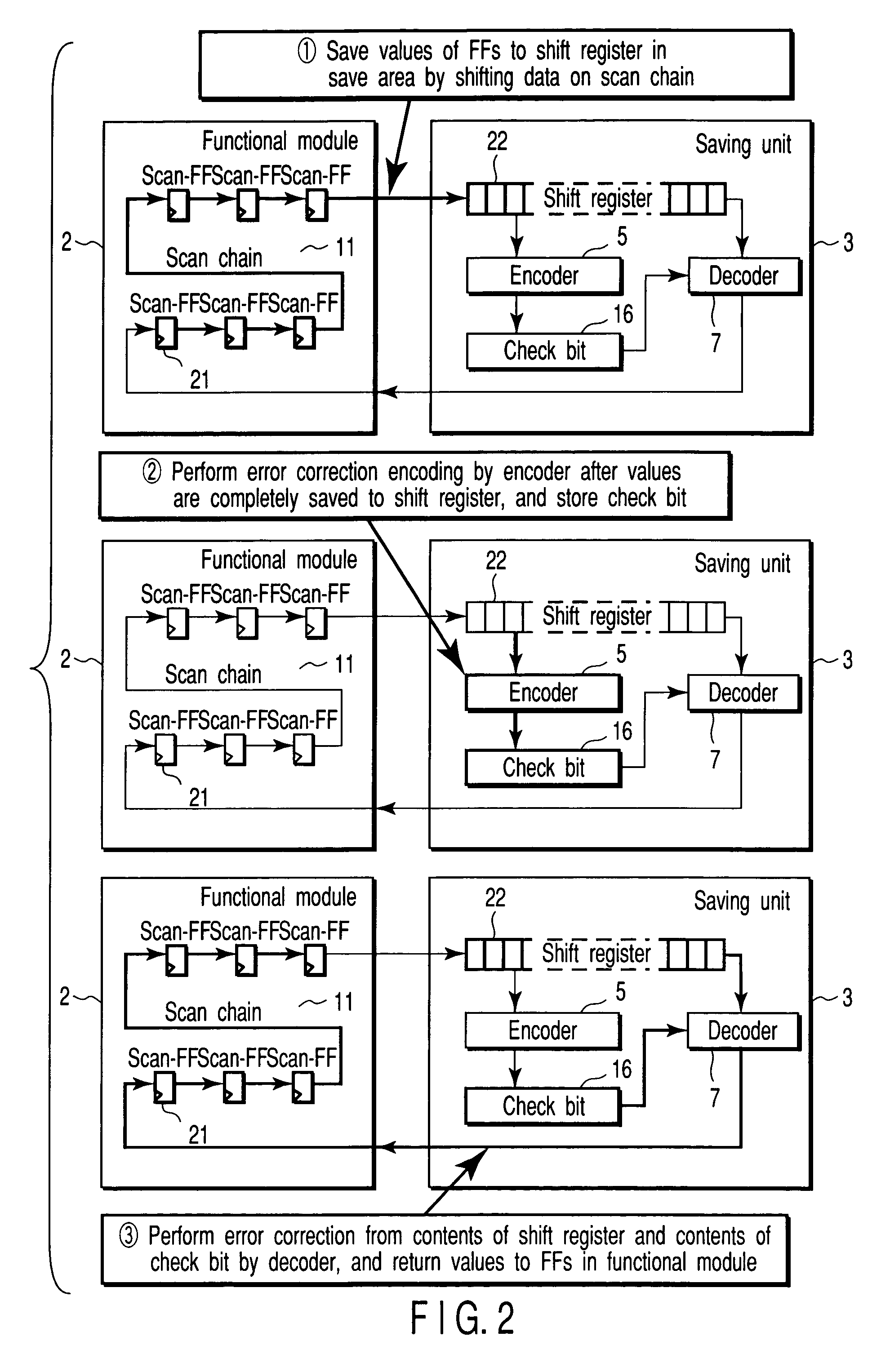
[0076]FIG. 7 is a block diagram showing the arrangement of a scan controller according to the second embodiment. A scan controller 10 of this embodiment includes a saving controller 30 which outputs enable signals (SH_EN_A and SH_EN_B) of a saving unit 3. The saving controller 30, not a PMU 1, is the main component of saving or restoration control. This is the difference from the configuration of the first embodiment described above.

[0077]Similar to that of the first embodiment, the scan controller 10 of this embodiment also switches the whole integrated circuit device to a scan test mode in a normal operation. When data saving or restoration by a shift operation using a scan chain 11 is to be performed, the saving controller 30 receives an instruction indicating this information from the PMU 1. In accordance with the instruction, the saving controller 30 selects a corresponding functional module and outputs the enable signal (SH_EN_A or SH_EN_B). Also, the saving controller 30 outp...

third embodiment

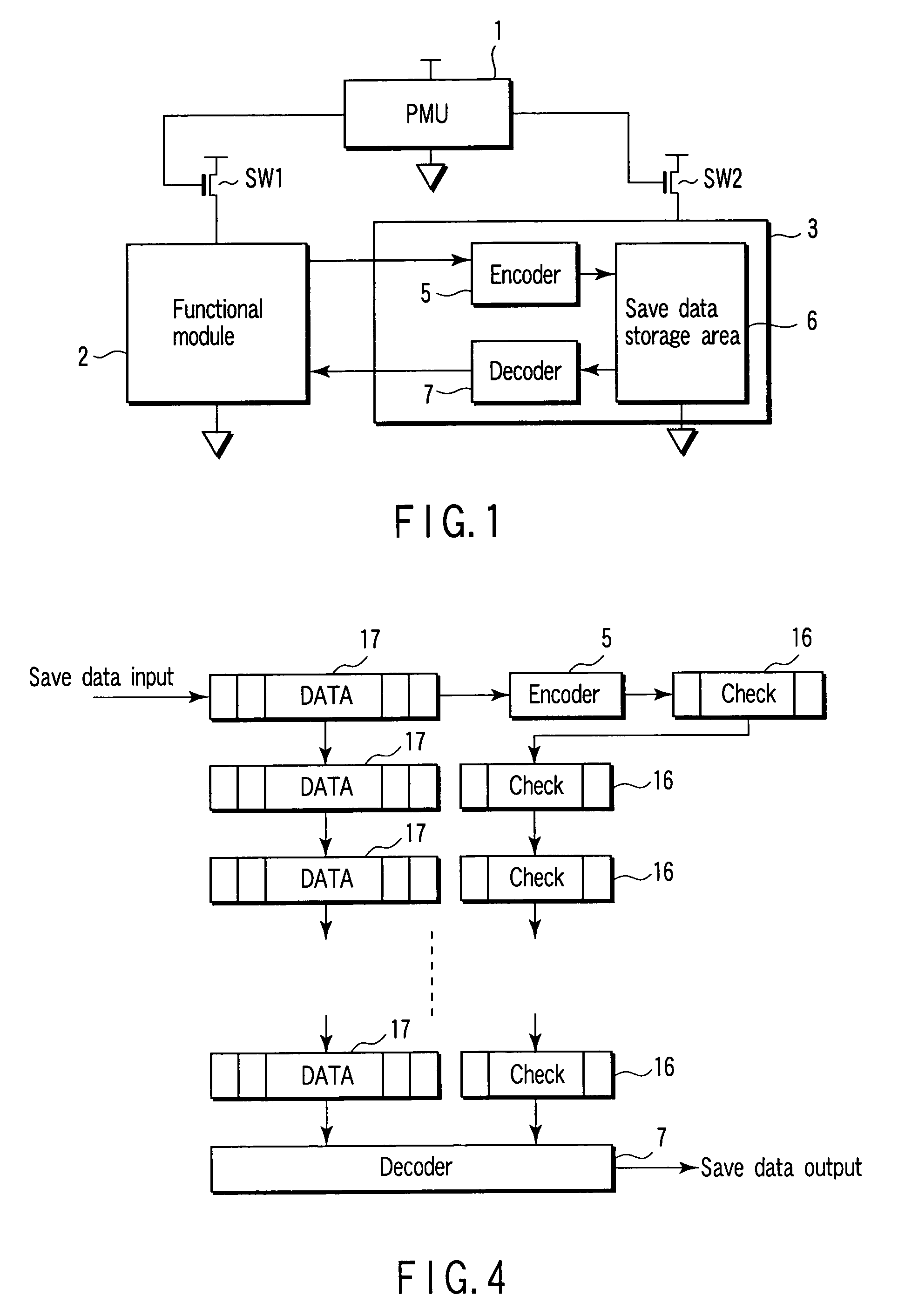
[0083]FIG. 9 is a block diagram showing the third embodiment (data is saved to a dedicated area) of the integrated circuit device according to the present invention.

[0084]Reference numeral 20 in FIG. 9 denotes a memory as a functional module. A module A for writing and reading out data in and from the memory 20 includes an address generator 23 which generates an address for accessing the memory 20.

[0085]A saving unit 3 has a save data storage area 6 as a dedicated area different from the memory 20 as a functional module. The saving unit 3 can be formed in each module or for a plurality of functional modules. If the capacity of the save data storage area 6 can be increased, a correction encoding process may be made unnecessary by the use of the majority method or the like. In this case, a serial-to-parallel converter and encoder 14 and a decoder and parallel-to-serial converter 15 can be omitted. An embodiment using the majority method will be explained later (the sixth embodiment).

[...


PUM


Abstract

An integrated circuit device includes at least one functional module which outputs save data in synchronism with a saving clock signal, a power supply control unit which selects one of the functional modules, and controls stop and resumption of power supply to the selected functional module, a save data storage unit which stores save data output from a functional module selected by the power supply control unit, and an error checking and correction unit which performs error checking and correction for the save data stored in the save data storage unit when the save data is to be restored to the functional module in synchronism with a restoration clock signal.

Description

CROSS-REFERENCE TO RELATED APPLICATIONS[0001]This application is based upon and claims the benefit of priority from the prior Japanese Patent Application No. 2002-289999, filed Oct. 2, 2002, the entire contents of which are incorporated herein by reference.BACKGROUND OF THE INVENTION[0002]1. Field of the Invention[0003]The present invention relates to an integrated circuit device in which power supply is controlled for individual functional modules in order to reduce power consumption, and saving and restoration of data in an internal register or the like is controlled.[0004]2. Description of the Related Art[0005]A conventional method of implementing a low-power system on a chip (SoC) is to stop the operation of a functional module in an idling state in order to reduce power consumption. Stopping the clock is known as a method of stopping the operation of a functional module. However, even when the operation of a functional module is stopped by stopping the clock, power is kept supp...

Claims


Application Information

Patent Timeline
IPC IPC(8): G11C29/00G01R31/28G06F1/30G06F1/32G06F11/00G06F12/16H03K19/00
CPCG06F1/3203G06F1/3237G06F1/324G06F1/3287G06F1/3296Y02B60/1285Y02B60/1217Y02B60/1221Y02B60/1282Y02D10/00
Inventor ARIMA, YUKIOISHIBASHI, KOICHIROYAMASHITA, TAKAHIRO
Owner SOCIONEXT INC
Why Eureka
Try Eureka