Method for producing chip stacks and chip stacks formed by integrated devices

a technology of integrated devices and chip stacks, which is applied in the direction of semiconductor devices, electrical equipment, semiconductor/solid-state device details, etc., can solve the problems of reduced electrical performance of the chip stack system, prone to electrical shorts of bond wires in conventional integrated device stacks, and more difficult handling and assembly of the integrated device stack

Inactive Publication Date: 2007-09-18
POLARIS INNOVATIONS LTD
View PDF4 Cites 13 Cited by
  • Summary
  • Abstract
  • Description
  • Claims
  • Application Information

AI Technical Summary

Benefits of technology

[0008]Therefore, one embodiment of the present invention provides a method for producing chip stacks wherein the provision of spacers as a distancing element between two stacked integrated devices can be avoided.
[0009]Furthermore, another embodiment of the present invention provides a method for producing chip stacks wherein the manufacturing of chip stacks can be facilitated.
[0010]A further embodiment of the present invention provides a chip stack with a reduced height which can be produced less expensively, the production time is reduced and the production yield is increased.

Problems solved by technology

In addition, the handling and the assembly of the integrated device stack is more challenging if the stack height is increased due to the provision of the spacers compared to stacks that do not comprise spacers.
Also, the length of the bond wires is higher in a chip stack having spacers than in a chip stack without spacers which leads to a reduced electrical performance of the chip stack system.
Moreover, conventional integrated device stacks are prone to produce electrical shorts of the bond wires while applying the spacer material and while positioning an integrated device onto the spacer material.
This reduces reliability and yield of production.

Method used


Image

  • Method for producing chip stacks and chip stacks formed by integrated devices
  • Method for producing chip stacks and chip stacks formed by integrated devices
  • Method for producing chip stacks and chip stacks formed by integrated devices

Examples


first embodiment

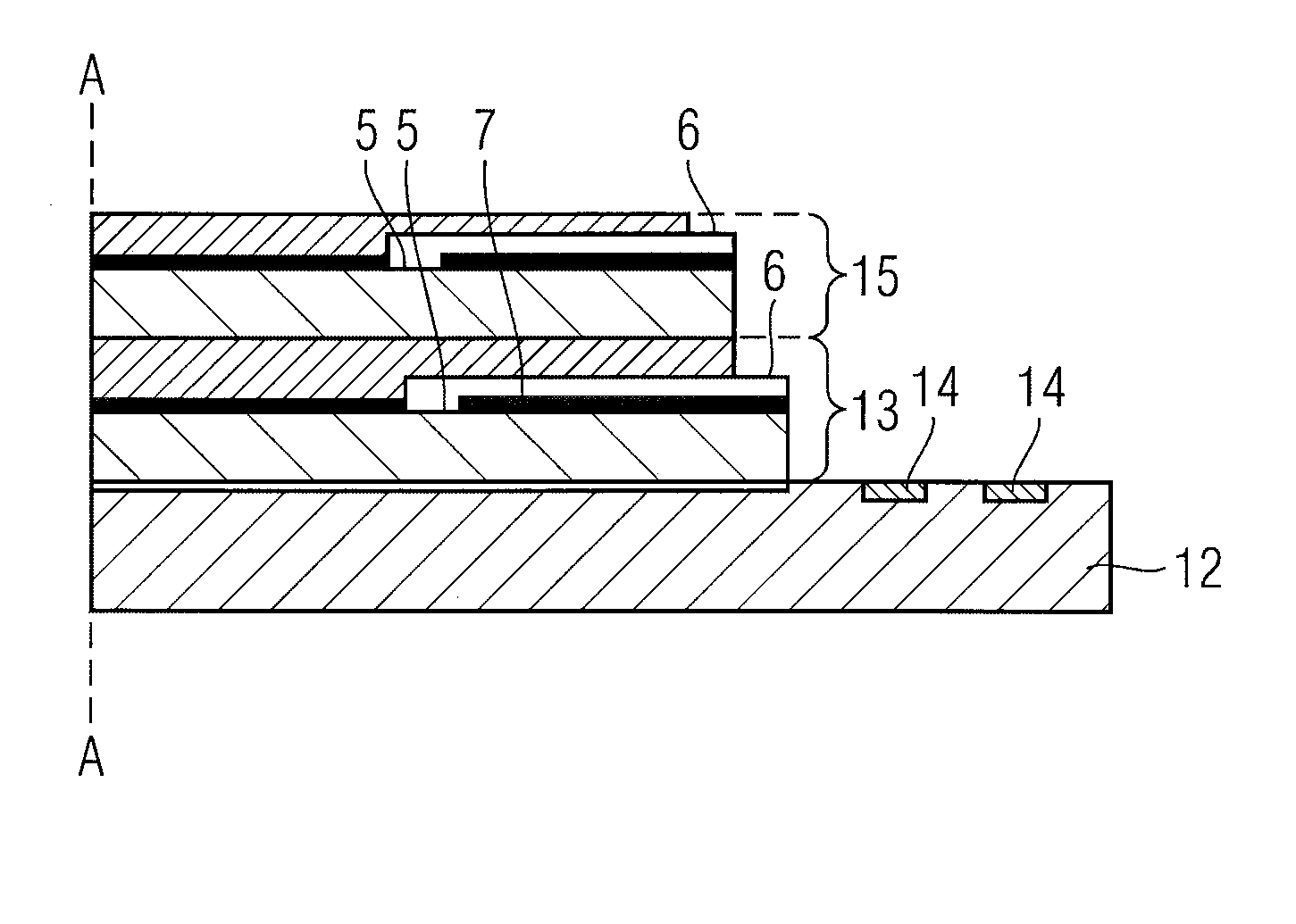
[0043]With regard to the FIGS. 1 to 8, the present invention is explained.

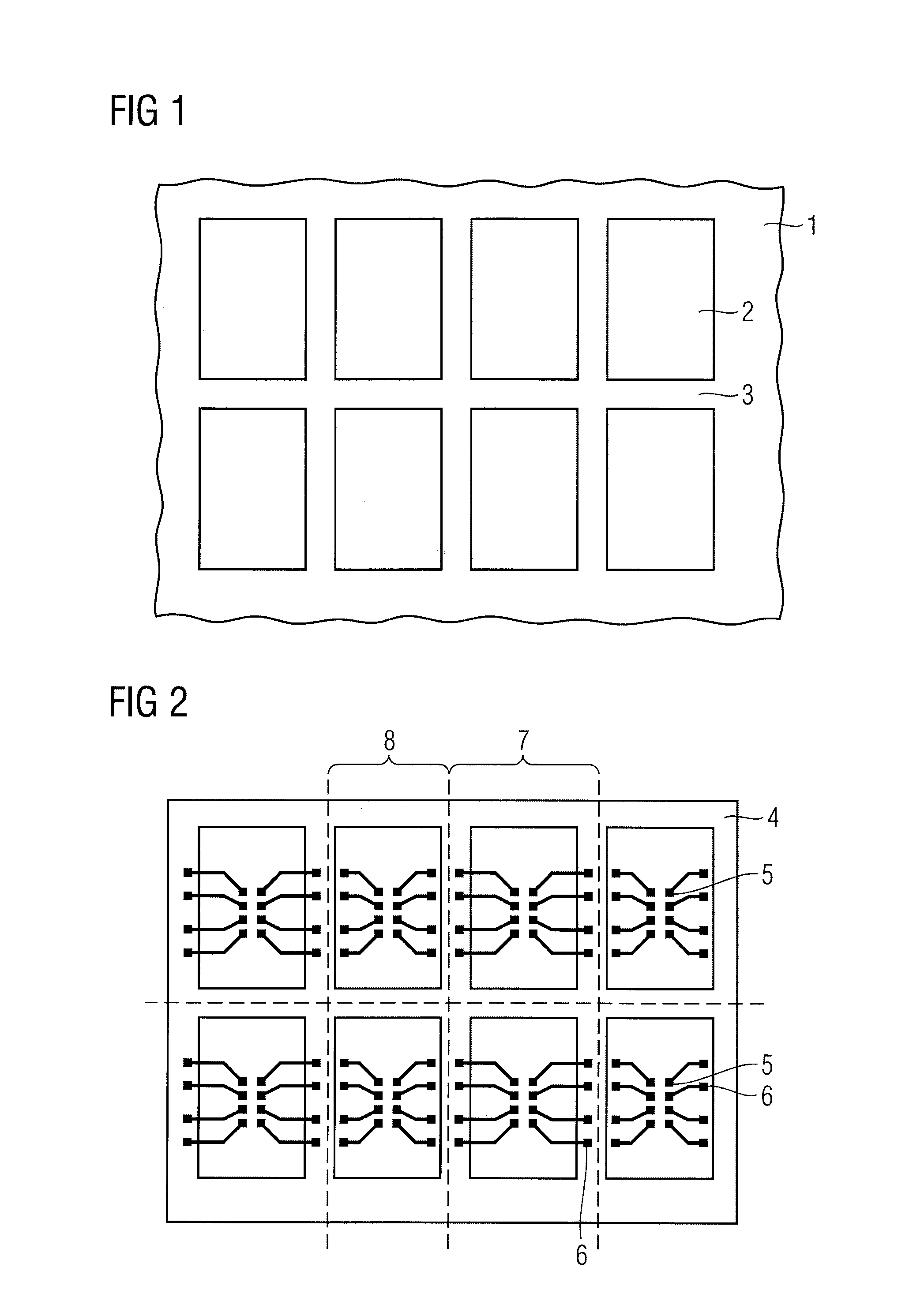
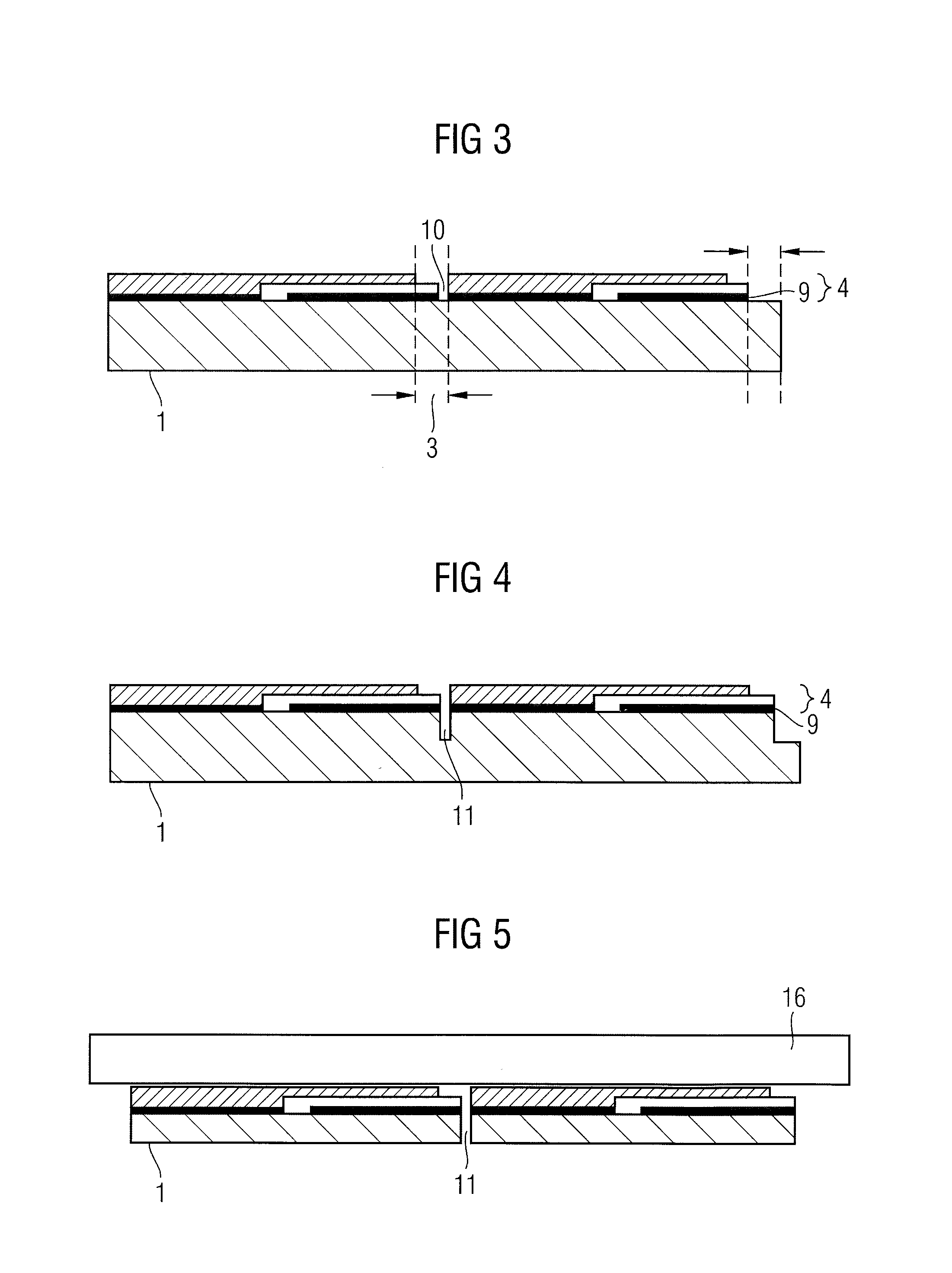
[0044]FIG. 1 shows a top view of a section of a single substrate 1 in which integrated structure areas 2 are provided. The integrated structure areas are applied in a regular arrangement. Each of the integrated structure areas is separated from a neighbored integrated structure area by a spacing which is herein called kerf area 3 as a kerf is usually located in this spacing when sawing the single substrate 1 in order to obtain separated integrated devices. The kerf area 3 normally has a width of 60 μm. Other kerf widths are possible, as well.

[0045]The integrated structure areas 2 include integrated structures, such as integrated circuits, microstructures and such like, and, hence, are also referred to herein as integrated circuit structures. Preferably, the integrated structure areas 2 each comprise the same structures, e.g. memory circuits, in one single substrate 1. The single substrate 1 may also include in...

second embodiment

[0058]With regard to the FIGS. 9 to 11, the present invention is explained. FIG. 9 shows a substrate 20 with a redistribution layer provided thereon, wherein the redistribution layer on a first integrated structure area 21 provides contact pads 25 in a first contacting area 23 which extend beyond the boundaries of the first integrated structure area 21 in a first horizontal orientation. A neighbored integrated device area includes the second integrated structure area 22 wherein the redistribution layer provides a second contacting area 24 having contact pads extending beyond the boundary of the second integrated structure area 22 in a second vertical orientation.

[0059]In the embodiment of FIG. 9, two types of integrated devices are to be produced wherein the two types of integrated device areas are preferably alternately arranged on the substrate. As the boundary of the integrated device area is not straight in this embodiment, sawing as a separation method is not appropriate, but a...


PUM


Abstract

The method of the present invention relates to a method for producing a chip stack comprising the steps of manufacturing at least a first and a second integrated structure on a single substrate, an area of the first integrated structure and an area of the second integrated structure adjoining a respective first and second kerf area; providing a first redistribution layer on the first integrated structure on the substrate, said first redistribution layer at least partially extending beyond the area of the first integrated structure into the first kerf area, thereby forming a first integrated device area, wherein a first contact pad is arranged on the first redistribution layer in a first contacting area overlapping the first kerf area; providing a second redistribution layer on a second integrated structure on the substrate, including a second contact pad, thereby forming a second integrated device area; separating the first and second integrated device areas along a separation line defined by at least one of the boundaries of the first integrated device area and the second integrated device area, resulting in separated first and second integrated devices; and stacking the second integrated device on the first integrated device so that the first contacting pattern is uncovered by the second integrated device.

Description

CROSS-REFERENCE TO RELATED APPLICATIONS[0001]This application is related to U.S. patent application Ser. No. 11 / 039,293, entitled SIGNAL REDISTRIBUTION USING BRIDGE LAYER FOR MULTICHIP MODULE, filed Jan. 20, 2005, by Thoai Thai Le et al., and U.S. patent application Ser. No. 11 / 208,362, entitled METHOD FOR MCP PACKAGING FOR BALANCED PERFORMANCE, filed Mar. 14, 2005, by Farid Barakat et al. Each of the aforementioned related patent applications is herein incorporated by reference in its entirety.BACKGROUND OF THE INVENTION[0002]1. Field of the Invention[0003]The present invention relates to a method for producing chip stacks and to chip stacks formed by stacked integrated devices.[0004]2. Description of the Related Art[0005]In order to further reduce the size of integrated systems, integrated devices, e.g., chips are arranged in stacks. Each of the integrated devices comprises contact pads thereon which are bonded to a system PCB (printed circuit board). In between the integrated dev...

Claims


Application Information

Patent Timeline
Patent Type & Authority Patents(United States)
IPC IPC(8): H01L21/44H01L21/48H01L21/50
CPCH01L25/0657H01L2224/48091H01L2224/48227H01L2225/0651H01L2225/06524H01L2225/06575H01L2924/00014
Inventor GROSS, HARALD
Owner POLARIS INNOVATIONS LTD
Why Eureka
Try Eureka