Lens and method for manufacturing same

a technology of optics and lenses, applied in optics, mountings, instruments, etc., can solve the problems of reducing image quality, poor optical performance, and reducing image quality, so as to reduce or completely avoid aberration-type astigmatism, reduce optical system costs, and simple design

Active Publication Date: 2012-06-07
FRAUNHOFER GESELLSCHAFT ZUR FOERDERUNG DER ANGEWANDTEN FORSCHUNG EV
View PDF4 Cites 7 Cited by
  • Summary
  • Abstract
  • Description
  • Claims
  • Application Information

AI Technical Summary

Benefits of technology

[0010]To overcome the problems outlined above with regard to the conventional wafer scale technology which necessitates the use of substrates to which the UV-polymer replicated lenses are applied the inventive approach avoids the provision of unnecessary material, e.g. glass, in the optical path.
[0011]In accordance with embodiments of the invention, lenses are manufactured by a multi-step sacrificial material process above one or more recesses or through holes in a substrate, e.g. a glass substrate. The conventional approach of directly forming the lenses on the surface(s) of a glass substrate is no longer pursued. The advantage of the inventive approach is that no “thick” glass is in the optical path. Thus, the lens thickness is substantially determined by the optic design which allows the use of much more advantageous lens shapes. Since the glass substrate outside the cavity of the imaging beam path is still maintained, also the overall mechanical stability of the arrangement is ensured.
[0012]Thus, when compared to conventional approaches the inventive approach is advantageous from an optical design perspective. Otherwise the substrate thickness introduces astigmatism into a convergent bundle so that in conventional wafer scale lens optical designs this had to be corrected by more elements and / or more complex lens shapes. Alternatively, one had to live with the poor optical performance. The substrate thickness increases TTL (TTL=total track length) since this means more than necessitated “high index material” in the optical path. The high index material, i.e. the material having a high refraction coefficient “n” (n about 1.5), increases the track to n*f (assuming 100% filling of the optical path with small n). Thus, the less the filling in the optical path is the less is the increase of thickness. In order to reduce TTL even with a thick substrate conventionally rays are bend outwards in front of the lens stack and bend back towards the optical axis close to the image sensor to reduce the CRA (CRA=chief ray angle). This results in high refractive power of the lenses, which is actually not needed but results in strong aberrations, which again have to be corrected by complex lens shapes, however, this results in unnecessary tight tolerances.
[0014]Applying the inventive approach avoids the need to provide substrates in the optical path. In accordance with the inventive design only the lens structure itself or only the optically useful part of the lens structure is within the optic path thereby avoiding the just mentioned problems.
[0016]An advantage of the inventive approach is that it is now possible to manufacture wafer scale lenses with a design which does no longer have to take into consideration the glass substrate. One further advantage is that by avoiding the optical unnecessary glass substrate (=parallel plates) within the convergent beam path the aberration type astigmatism is reduced or completely avoided. Thus, it is no longer necessary to correct possible image errors by additional measures and / or lenses having a complicated design. This results in a more simple design and reduces costs for the optical system.

Problems solved by technology

This approach is disadvantageous as for mechanical and structural reasons the amount of high refractive index material, i.e. materials having a refractive index n of about 1.5 vs. n=1 of air, (e.g. the substrates which form parallel plates) within the imaging beam path is higher as it is desired by the optical design.
This reduces the image quality and necessitates more lenses and / or lenses having a more complicated shape within the stack to compensate for the reduced image quality.
Thus, the adaptation of “classic” lens designs and the use of the design rules which apply for these classic lens designs which avoid the occurrence of specific imaging errors cannot be used in the design of such wafer scale lenses.
However, this is contradiction to lens arrangements observed in classical objective designs where for example arrangements of one or several thin but strongly bent meniscuses are applied in order to reduce aberrations and especially to obtain a small astigmatism.
This is a drawback of state-of-the-art wafer scale lens designs as due to the evident problem of astigmatism in these designs their optical performance is poor although much more complex (highly aspheric) lens shapes are applied.
The problem of thick substrates is especially evident for the above mentioned meniscus lenses, which is the lens that has lens surfaces which are curved into the same direction.
However, this approach is disadvantageous, as the wafer itself is not a stable support device (e.g. a stable glass support).
This instable support will result in inhomogeneities regarding the thickness and the bending of the wafer.
Also shrinkage of the wafer is observed resulting in a lateral uncertainty.
These effects can be severe such that a plurality of wafers or plates cannot be stacked on top of each other.
However, the procedural overhead for generating lenses using injection molding in terms of machinery and in terms of process steps is disadvantageous.
Further, no manufacturing on a wafer scale is possible.
Alternatively, one had to live with the poor optical performance.
This results in high refractive power of the lenses, which is actually not needed but results in strong aberrations, which again have to be corrected by complex lens shapes, however, this results in unnecessary tight tolerances.
In case substrates are necessitated in between these surface that means that the center thickness of the lens will be very high with the above mentioned problems as a consequence.

Method used


Image

  • Lens and method for manufacturing same
  • Lens and method for manufacturing same
  • Lens and method for manufacturing same

Examples


Embodiment Construction

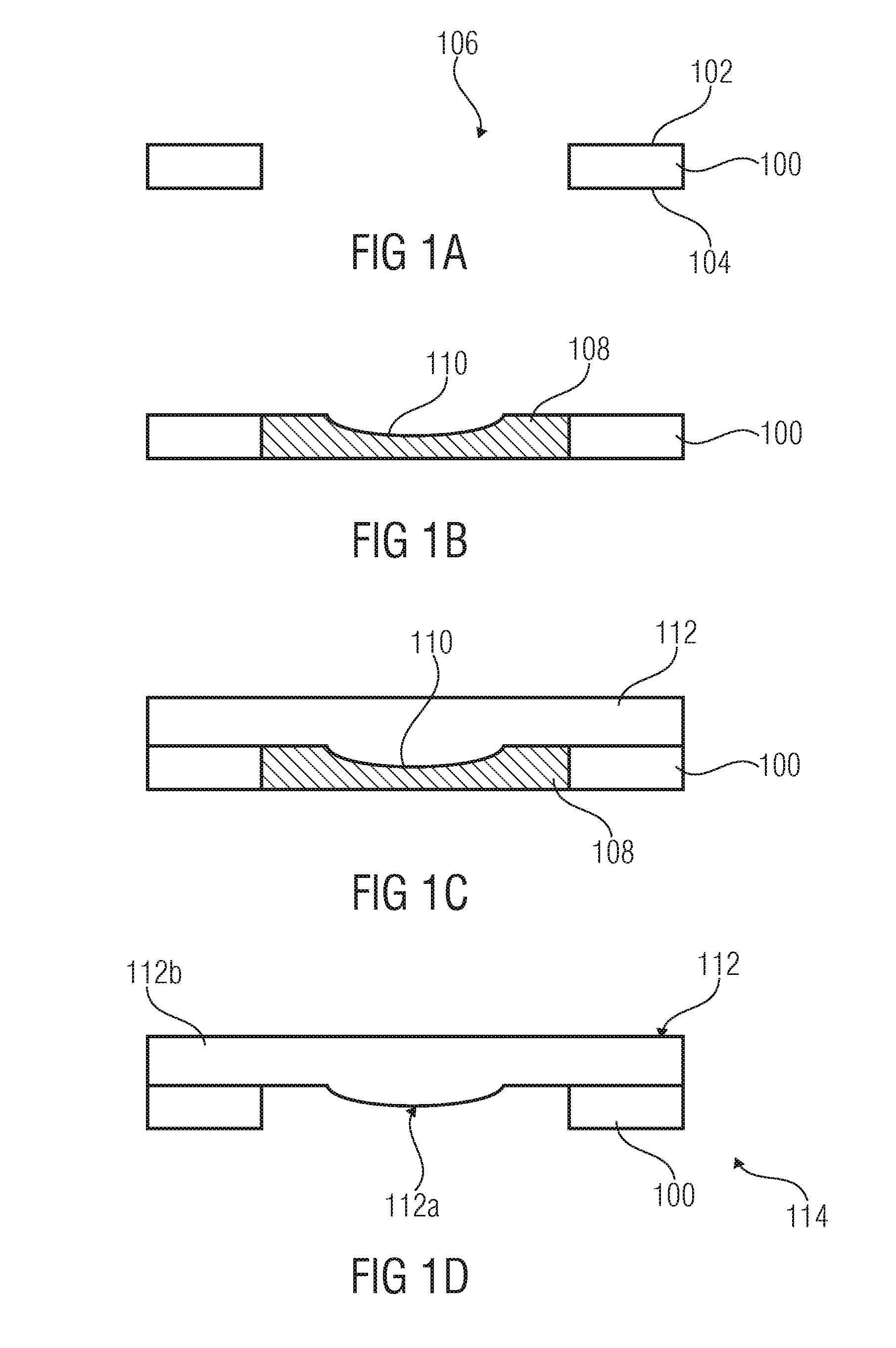
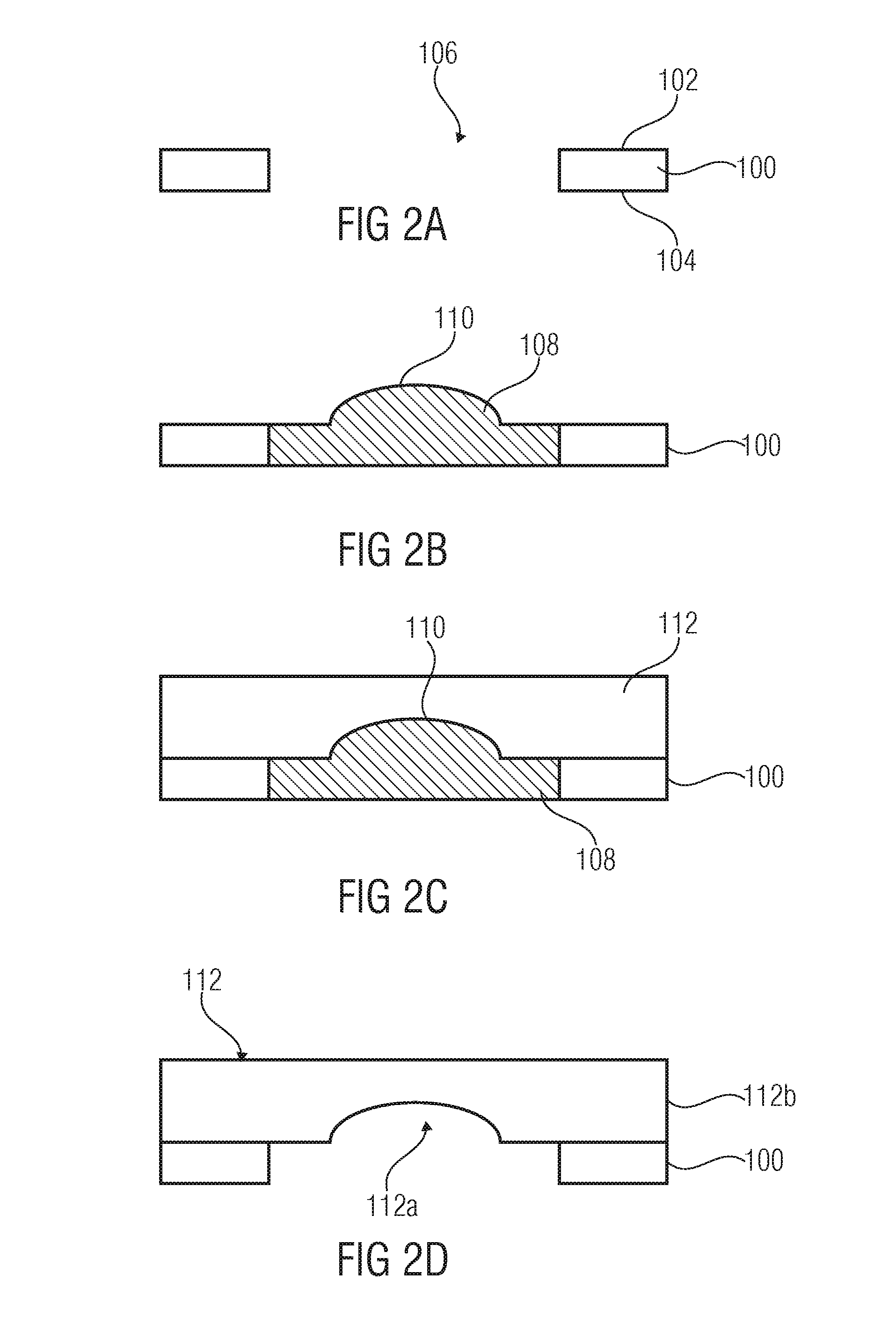
[0028]FIG. 1 shows an embodiment for manufacturing a plano convex lens.

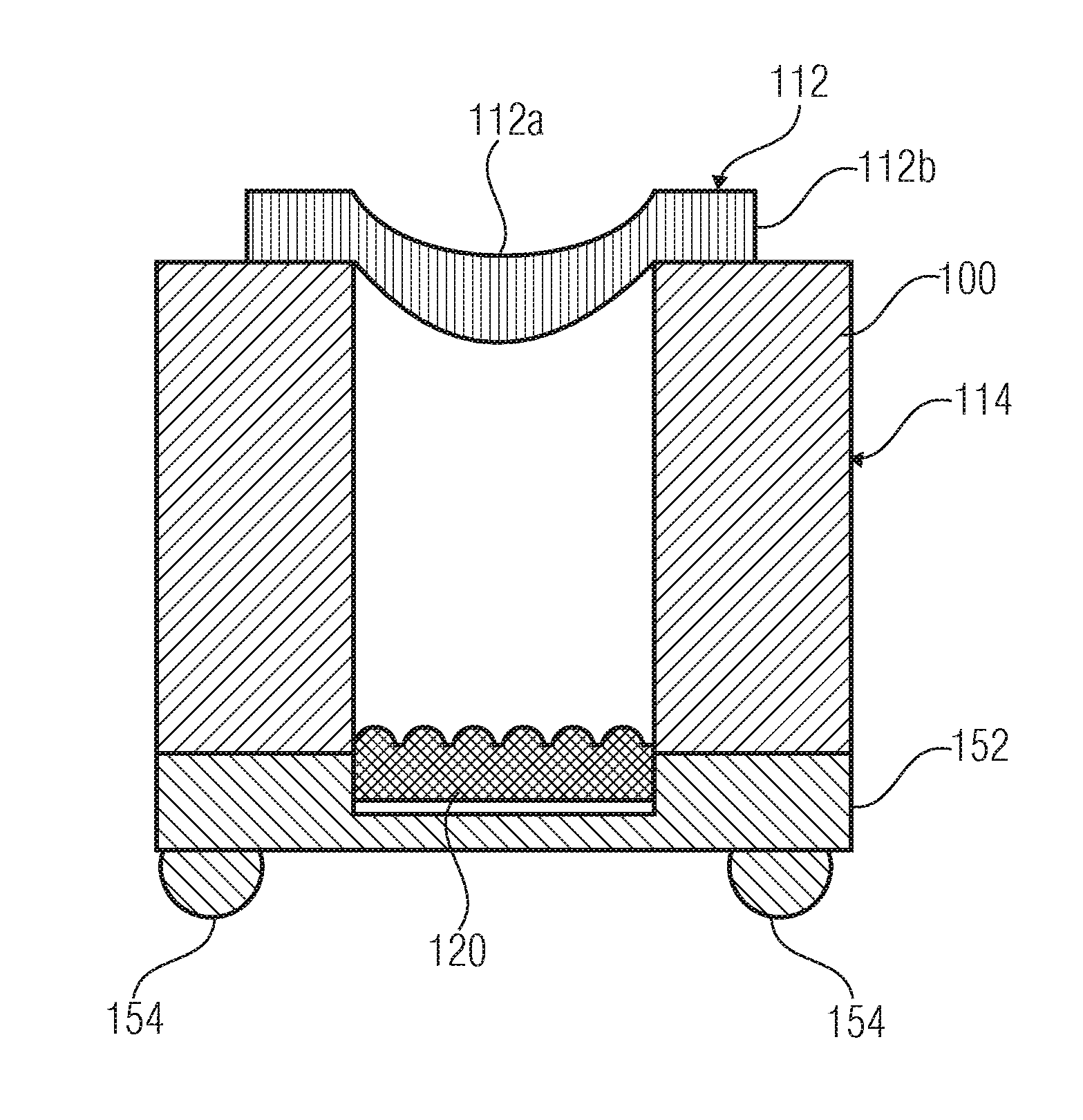
[0029]As is shown in FIG. 1(a) a substrate 100 is provided, which is shown in a cross-sectional view and comprises two opposing surfaces 102 and 104 and a recess 106 formed in the upper surface 102 of the substrate 100 and extending through the thickness of the substrate 100 to the lower surface 104 of the substrate 100 thereby defining a hole through the substrate 100. The hole in the substrate 100 is temporarily filled with a solvable polymer (a sacrificial material) 108 (see FIG. 1(b)). The polymer may be a solvent (e.g. acetone or isopropanole)-soluble polymer, like a conventional photoresist or a special water-soluble polymer / photoresist (typically on a polyvenylalcohole-basis). A portion 110 of the polymer 108 is shaped in accordance with a first desired lens surface. The portion 110 is only shaped into the polymer material 108 within the recess 108.

[0030]A final UV-polymer 112 (which may be an organic-inor...


PUM

PropertyMeasurementUnit
refractive indexaaaaaaaaaa
thicknessaaaaaaaaaa
shapeaaaaaaaaaa

Abstract

In a method for manufacturing a lens, a substrate which has a recess in a first surface thereof is provided. A sacrificial material is provided in the recess which has shape in accordance with a first desired lens surface. A lens material is applied to the substrate and to the sacrificial material and cured so that the lens material has a shape in accordance with the first desired lens surface, and then the sacrificial material is removed.

Description

[0001]Embodiments of the invention concern the field of optical systems, more specifically the field of lenses and manufacturing such lenses. Embodiments of the invention relate to wafer scale optics, more specifically to wafer scale lens designs that may be used in lens arrangements or optical systems, e.g. in digital cameras in mobile phones, personal digital assistants and the like, especially in combination with CMOS image sensors.BACKGROUND OF THE INVENTION[0002]In the field of wafer scale optics lenses are manufactured by providing a UV curable polymer material onto a thick glass substrate and shaping the polymer material into a desired lens form. The polymer may be deposited either on one side or on both sides of the glass substrate. A plurality of such lens wafers are stacked on each other, either directly or by means of one or more spacer wafers which may be glass or polymer substrates comprising holes. Thus, the respective lenses are arranged with a distance to the imaging...

Claims


Application Information

Patent Timeline
Patent Type & Authority Applications(United States)
IPC IPC(8): G02B7/02B29D11/00
CPCB29D11/00375
Inventor DUPARRE, JACQUESOLIVER, STEVEN
Owner FRAUNHOFER GESELLSCHAFT ZUR FOERDERUNG DER ANGEWANDTEN FORSCHUNG EV
Why Eureka
Try Eureka