Method for fabricating chip package

a chip and chip technology, applied in the direction of electrical equipment, semiconductor devices, semiconductor/solid-state device details, etc., can solve the problems of increasing signal delay and attenuation, reducing increasing signal path distances, so as to increase signal path distances, and reduce the distance of signal transmission paths

Inactive Publication Date: 2007-09-18
QUALCOMM INC
View PDF12 Cites 54 Cited by
  • Summary
  • Abstract
  • Description
  • Claims
  • Application Information

AI Technical Summary

Problems solved by technology

As a result, this method fails to reduce the distance of the signal transmission path but in fact increase the signal path distance.
This will increase signal delay and attenuation and decrease the performance of the chip.
Although WLCSP can greatly reduce the signal path distance, it is still very difficult to accommodate all the bonding points on the die surface as the integration of die and internal devices gets higher.
The pin count on the die increases as integration gets higher so the redistribution of pins in an area array is difficult to achieve.
Even if the redistribution of pins is successful, the distance between pins will be too small to meet the pitch of a printed circuit board (PCB).

Method used


Image

  • Method for fabricating chip package
  • Method for fabricating chip package
  • Method for fabricating chip package

Examples


first embodiment

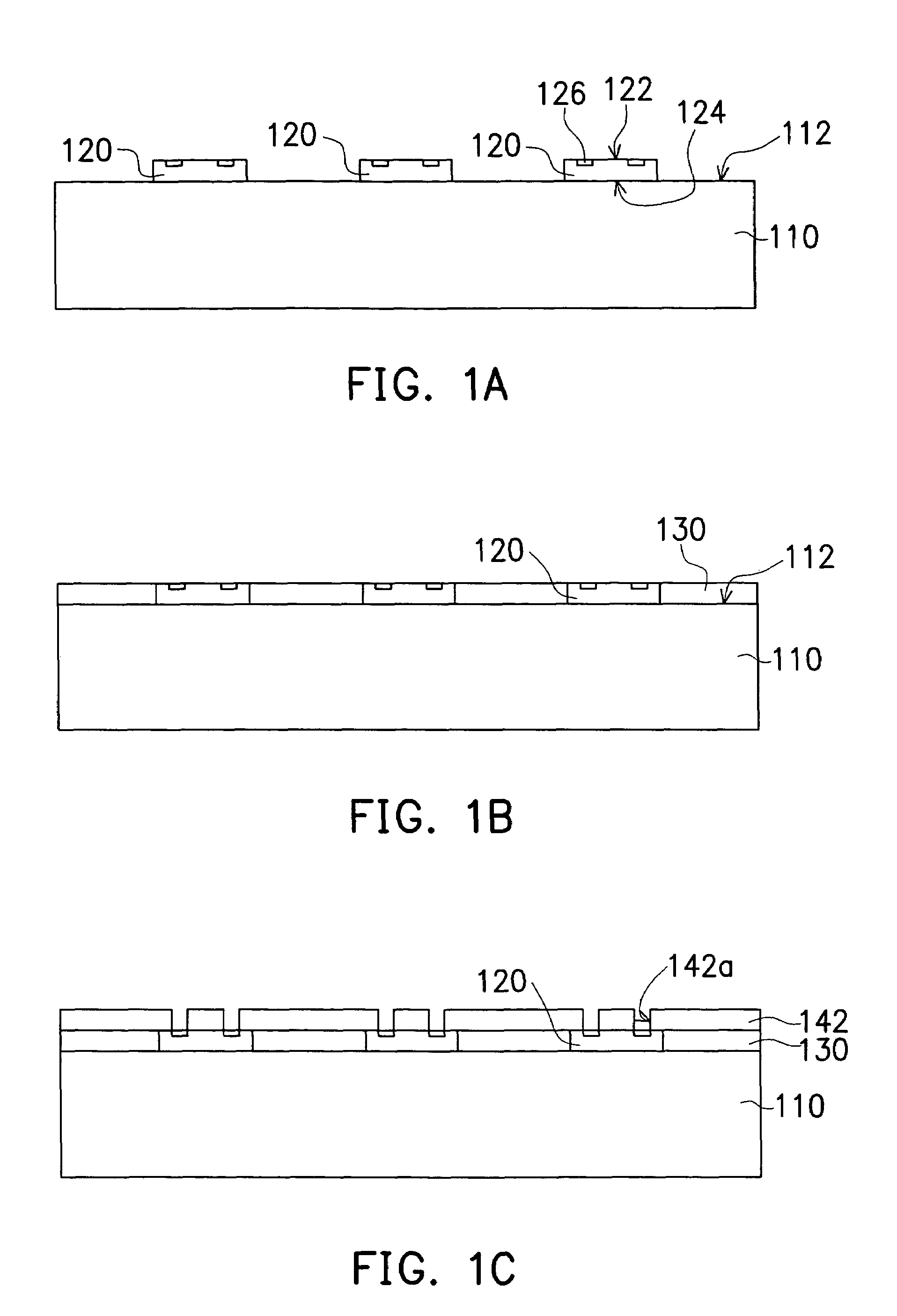
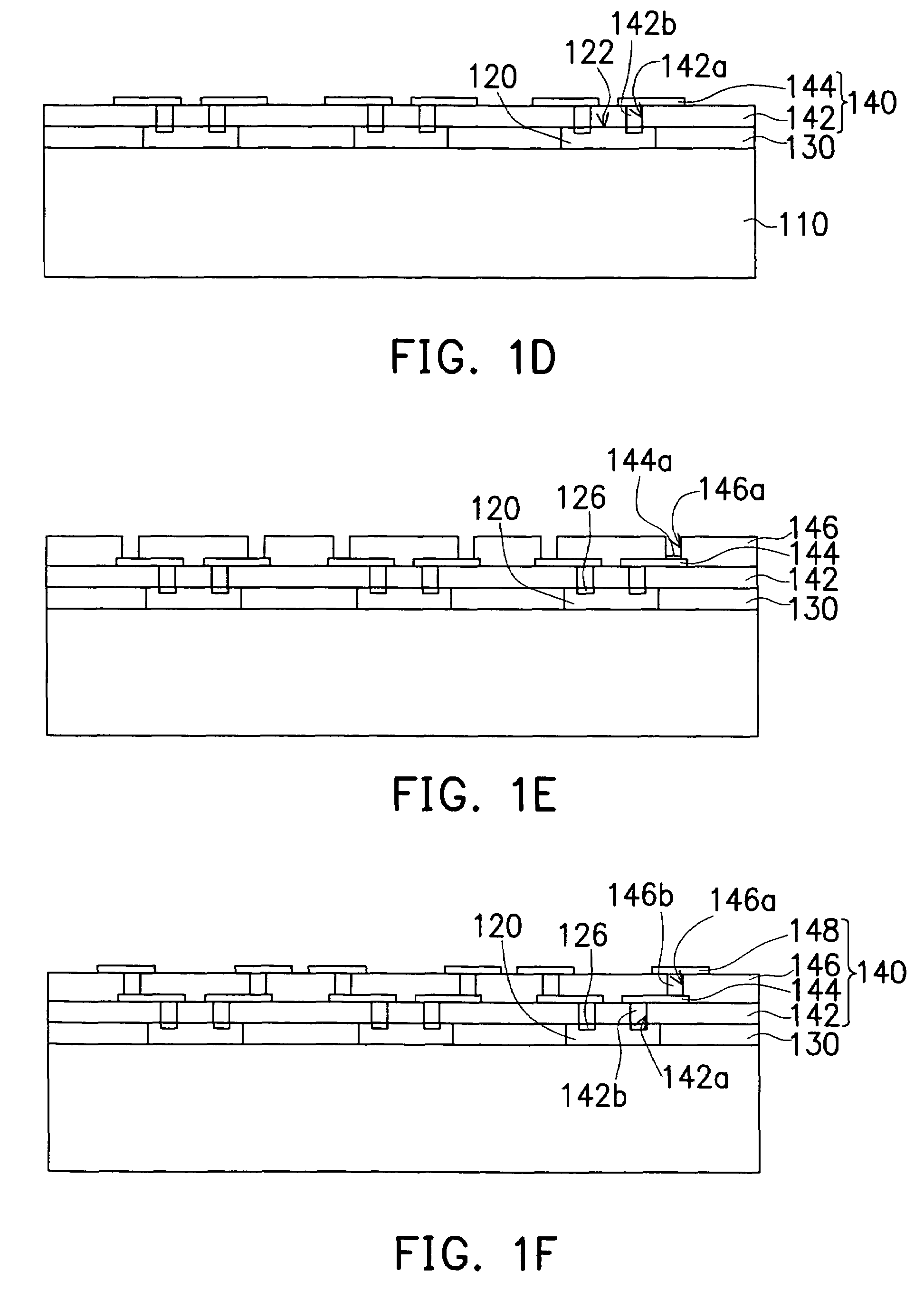
[0041]According to the above, the present invention is a chip package structure with a metal substrate and a plurality dies on it. The external circuitry of the thin-film circuit layer allows the metal pads of the die to fan out. By forming bonding pads corresponding to the metal pads of the dies such as solders balls, bumps, or pins as the signal input terminals, the distance of the signal path is effectively decreased. As a result, signal delay and attenuation is reduced to increase performance of the die.

[0042]Furthermore, the dies are directly touching the metal substrate, which helps the chips dissipate the high heat generated during operation because of the high heat conductivity of metal. Performance of the chip will thereby be increased. Moreover the fabrication technique on metal substrate is already well known in the art and the cost of metal is low, the present invention can effectively lower the cost of chip packaging and also increase performance of the chip by providin...
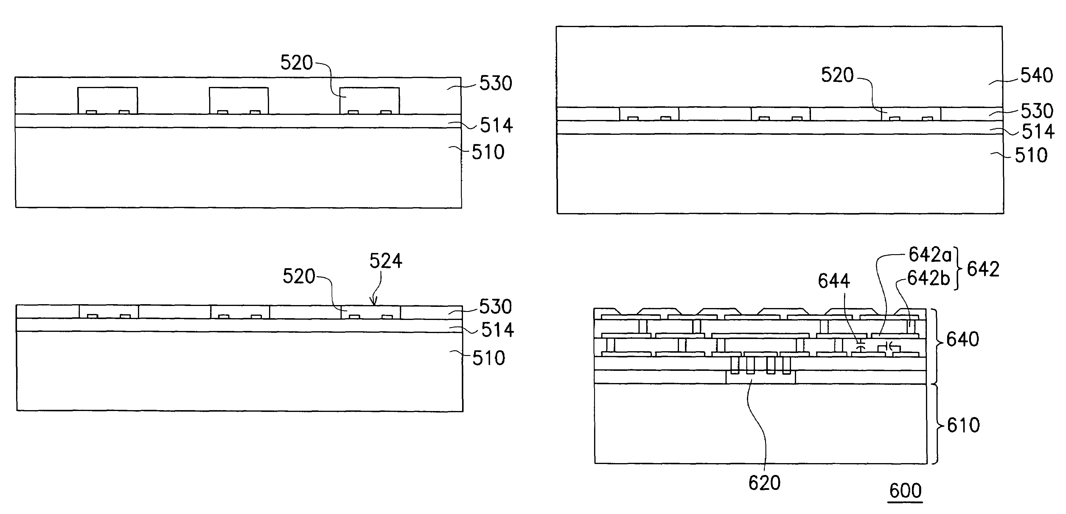
second embodiment

[0046]the present invention is a metal substrate with a plurality of inwardly protruded areas for inlaying dies by adhering the backside of the dies to the bottom of the inwardly protruded areas and exposing the active surface of the dies. A thin-film circuit layer is formed on top of the dies and the metal substrate to fan out the metal pads of the dies by using the external circuitry of the thin-film circuit layer. Due to the inlay of the dies in the metal substrate, thinning of the thickness of the chip package structure is effectively achieved and the surface of the metal substrate provides enough planarity and support for the formation of the thin-film circuit layer.

third embodiment

[0047]the present invention differs from the second embodiment of the present invention by using an alloy metal substrate. FIG. 3A to 3C are schematic diagrams of the sectional view of the third embodiment illustrating the fabrication of the structure.

[0048]Please refer to FIG. 3A, a metal substrate 310 is constructed with a first metal layer 310a and a second metal layer 310b. A surface 312 of metal substrate 310 is the face of second metal layer 310b that is further away from first metal layer 310a. A plurality of openings 314a is formed on first metal layer 310a by punching and the thickness of first metal layer 310a is approximately equal to that of dies 320 so the depth of openings 314a is approximately equal to the thickness of dies 320.

[0049]In FIG. 3B, first metal layer 310a is placed overlapping second metal layer 310b so openings 314a of first metal layer 310a form inwardly protruded areas 314 on the surface of second metal layer 310b. Following in FIG. 3C, backside 324 of...


PUM


Abstract

An integrated chip package structure and method of manufacturing the same is by adhering dies on a metal substrate and forming a thin-film circuit layer on top of the dies and the metal substrate. Wherein the thin-film circuit layer has an external circuitry, which is electrically connected to the metal pads of the dies, that extends to a region outside the active surface of the dies for fanning out the metal pads of the dies. Furthermore, a plurality of active devices and an internal circuitry is located on the active surface of the dies. Signal for the active devices are transmitted through the internal circuitry to the external circuitry and from the external circuitry through the internal circuitry back to other active devices. Moreover, the chip package structure allows multiple dies with different functions to be packaged into an integrated package and electrically connecting the dies by the external circuitry.

Description

CROSS-REFERENCE TO RELATED APPLICATION[0001]This application claims the priority benefit of Taiwan application serial no. 90133194, filed Dec. 31, 2001. This application is a divisional application of, and claims the priority benefit of U.S. application Ser. No. 10 / 055,560 filed on Jan. 22, 2002.[0002]This application is related to application Ser. No. 10 / 054,001, filed on Jan. 19, 2002, now U.S. Pat. No. 6,673,698; and related to application Ser. No. 10 / 690,350, filed on Oct. 21, 2003, now pending; and related to application Ser. No. 10 / 996,535, filed on Nov. 24, 2004, now pending; and related to application Ser. No. 10 / 996,537, filed on Nov. 24, 2004, now pending; and related to application Ser. No. 10 / 055,498, filed on Jan. 22, 2002, now U.S. Pat. No. 6,800,941; and related to application Ser. No. 10 / 454,972, filed on Jun. 4, 2003, now pending; and related to application Ser. No. 10 / 638,018, filed on Aug. 8, 2003, now pending; and related to application Ser. No. 10 / 055,568, filed...

Claims


Application Information

Patent Timeline
Patent Type & Authority Patents(United States)
IPC IPC(8): H01L21/00H01L23/34H01L21/60H01L23/31H01L23/36H01L23/498H01L23/538
CPCH01L23/3114H01L23/49816H01L23/49822H01L23/5389H01L24/19H01L24/97H01L23/36H01L2224/0401H01L2224/04105H01L2224/20H01L2224/211H01L2224/97H01L2924/01013H01L2924/01029H01L2924/01078H01L2924/01079H01L2924/09701H01L2924/14H01L2924/15153H01L2924/15165H01L2924/15174H01L2924/15311H01L2924/15787H01L2924/19041H01L2924/19042H01L2924/19043H01L2224/92244H01L2224/73267H01L2224/32225H01L2224/24137H01L2224/12105H01L2924/01005H01L2924/01023H01L2924/01033H01L2224/82H01L2224/83H01L21/568H01L2224/32245H01L2924/12042H01L2924/15747H01L2924/00
Inventor LIN, MOU-SHIUNGLEE, JIN-YUANHUANG, CHING-CHENG
Owner QUALCOMM INC
Why Eureka
Try Eureka