Method of manufacturing a semiconductor device having adjoining substrates

a manufacturing method and semiconductor technology, applied in the direction of optics, transistors, instruments, etc., can solve the problems of increasing the need for enlarge the related manufacturing device, the expansion and contraction of the substrate is considerable, and the difficulty of accurately positioning the element chip, etc., to achieve the effect of convenient application

Inactive Publication Date: 2006-09-05
SAMSUNG ELECTRONICS CO LTD
View PDF15 Cites 18 Cited by
  • Summary
  • Abstract
  • Description
  • Claims
  • Application Information

AI Technical Summary

Benefits of technology

[0009]Accordingly, an object of the present invention is to provide technology for facilitating the manufacture of a semiconductor device or electro-optic device of a large size substrate by employing the stripping-transcription technology.
[0072]Preferably, the foregoing thin film element is a thin film transistor or an organic electroluminescence element. Stripping and transcription can be applied easily to a thin film element or a thin film circuit.

Problems solved by technology

Nevertheless, when employing a large size substrate as the subject to be transcribed, it is unexpectedly difficult to accurately position the element chip, which is the transcriptional target, and such substrate.
In particular, with a print substrate or flexible print circuit, the expansion and contraction of the substrate is considerable.
Further, when the substrate of the subject to be transcribed becomes a large size, it becomes necessary to enlarge the related manufacturing device.
When the substrate becomes a large size, handling during the manufacture also becomes difficult.

Method used


Image

  • Method of manufacturing a semiconductor device having adjoining substrates
  • Method of manufacturing a semiconductor device having adjoining substrates
  • Method of manufacturing a semiconductor device having adjoining substrates

Examples


first embodiment

[0094](First Embodiment)

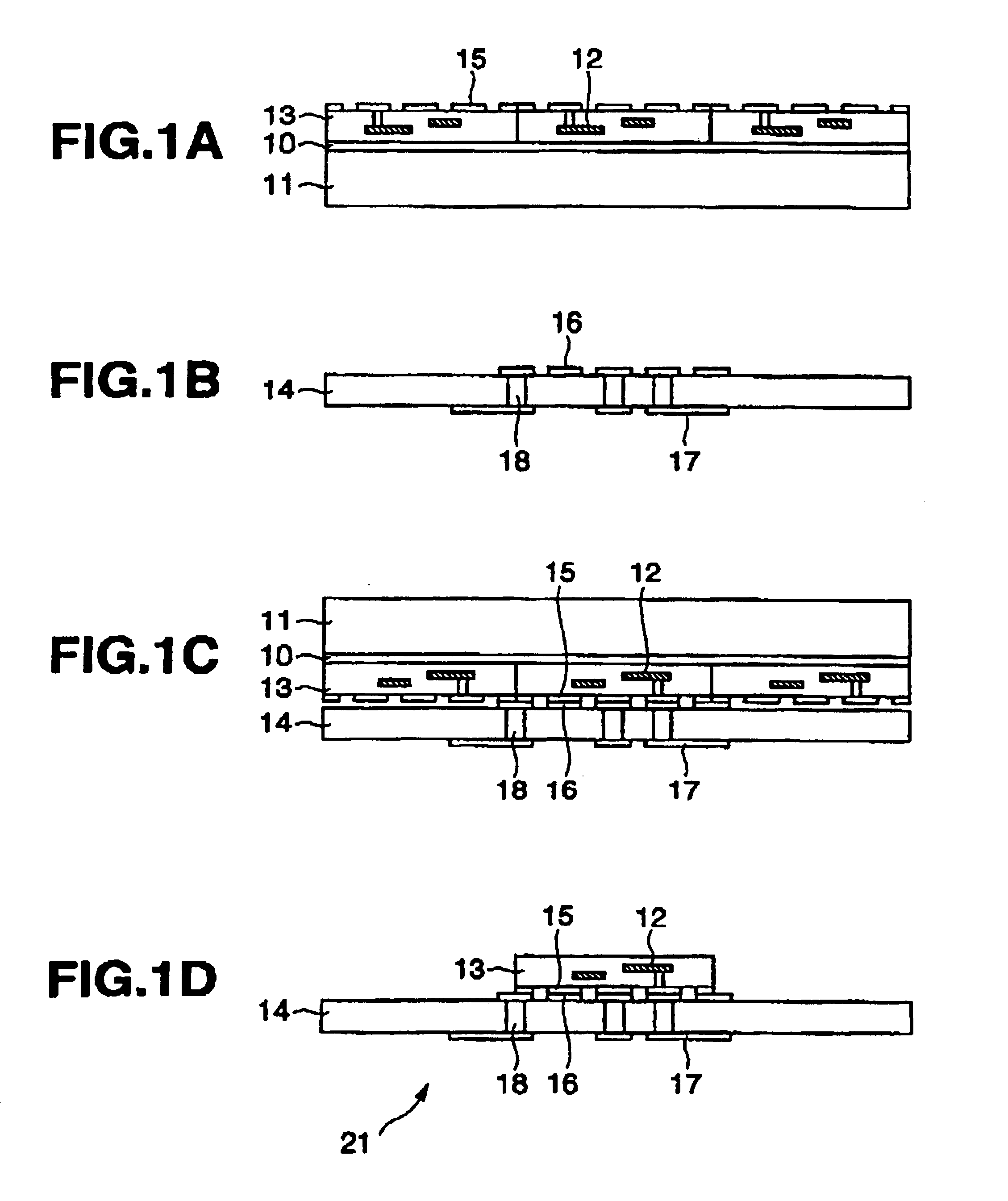
[0095]FIG. 1 is a process chart for explaining the manufacturing process of the semiconductor device of the first embodiment according to the present invention.

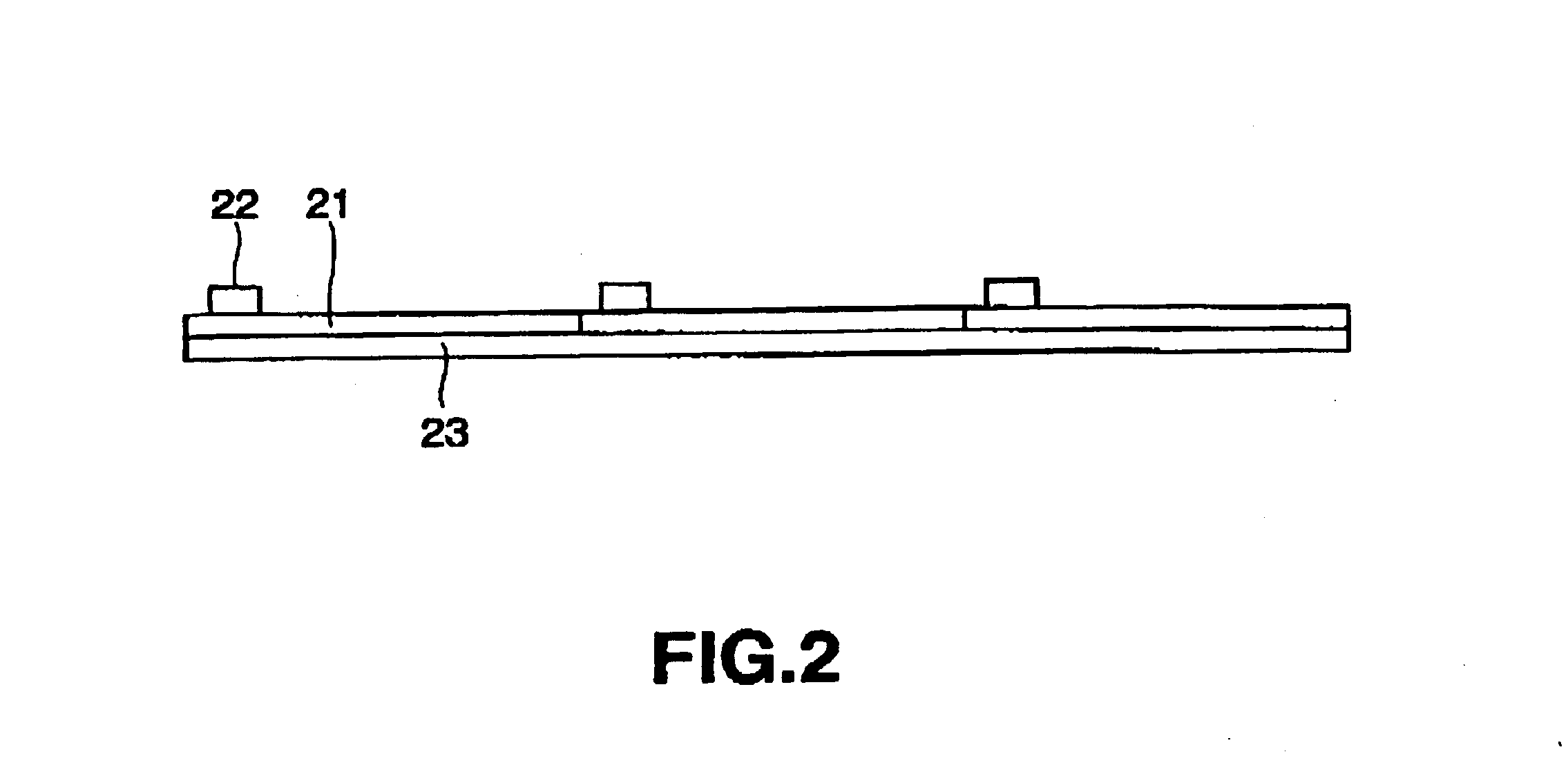
[0096]Foremost, as shown in FIG. 1A, a plurality of function element chips 13 containing one or more function elements 12 is formed on a transparent first substrate 11 such as a quartz glass via a stripping layer 10 such as amorphous silicon. A first pad 15 formed of a conductive material is formed on the respective function element chips 13 as a terminal for circuit connection.

[0097]FIG. 1B shows the second substrate to which the function element chip 13 is to be transcribed. The second substrate 14 is, for example, a print wiring circuit substrate, and formed on the upper face thereof is a second pad 16 formed of a conductive material, and formed on the lower face thereof are a wiring 17, and a via plug 18 (conductive material for filling in the via holes) for connecting the second pad 16 and the wir...

second embodiment

[0106](Second Embodiment)

[0107]FIG. 3A to FIG. 3E are process charts for explaining the manufacturing process of the semiconductor device of the second embodiment according to the present invention. In this example, a third substrate (temporary transcription substrate) is used.

[0108]Foremost, as shown in FIG. 3A, a stripping layer 10 such as amorphous silicon is formed on a transparent first substrate 11 such as a quartz glass. Then, a plurality of function element chips 13 containing one or more function elements 12 is formed thereon.

[0109]As shown in FIG. 3B, a temporary adhesive layer 19a is formed on the third substrate 19 as a temporary transcription substrate.

[0110]As shown in FIG. 3C, the first substrate 11 and the third substrate 19 are attached to each other via the temporary adhesive layer 19a. An abrasion is generated upon irradiating laser from the back face of the first substrate 11 onto the stripping layer 10 of the bedding of the function element chip 13, which is to ...

third embodiment

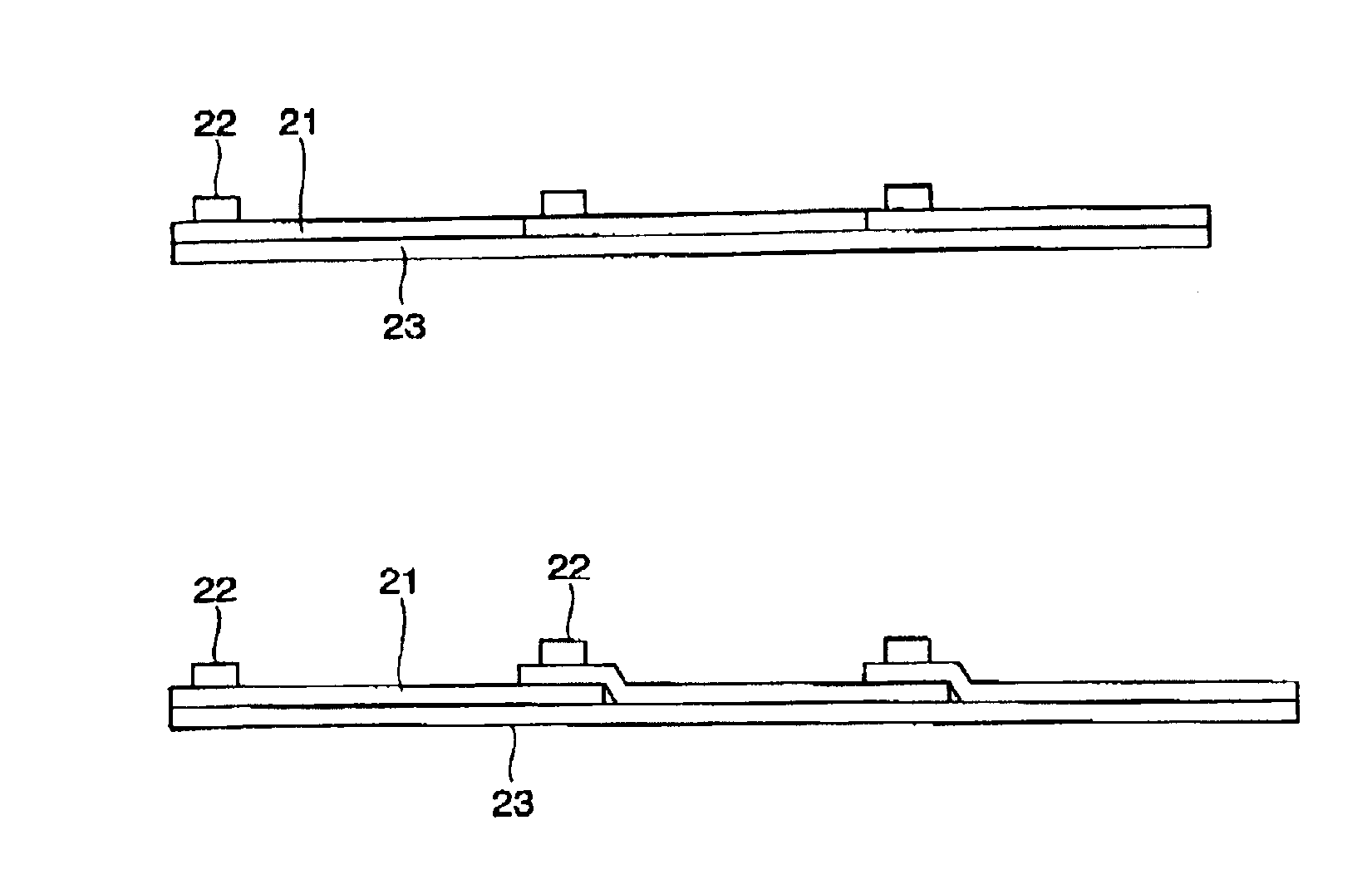
[0117](Third Embodiment)

[0118]FIG. 5 is a diagram showing the structure of the semiconductor device of the third embodiment according to the present invention. The chip-transcribed second substrate 21 and the manufacturing process thereof are approximately the same as the first and second embodiments described above.

[0119]In the present embodiment, the circuits mounted between the plurality of chip-transcribed second substrates 21 are mutually connected. Moreover, the chip-transcribed second substrates 21 disposed in a tile shape area attached to a single fourth substrate 24, and the circuit on the second substrate 21 is connected thereto via the anisotropic conductive material 25 and connection wiring 26 formed on the fourth substrate 24. Further, the support substrate 23 may also serve as the fourth substrate 24. Here, it is preferable that a concave portion is provided such that a connection wiring 26 can be formed on the fourth substrate 24. Thereupon, the center of the concave ...


PUM

PropertyMeasurementUnit
electricallyaaaaaaaaaa
electric fieldaaaaaaaaaa
sizeaaaaaaaaaa

Abstract

The present invention aims to manufacture a large size semiconductor device with the inter-substrate transcription technology of thin film circuits. Enlargement is enabled by disposing a plurality of second substrates (21) in a tile shape. As the second substrate (21), a print substrate or flexible print circuit having double-sided wiring or multilayer wiring is employed. The plurality of second substrates (21) is driven independently, and the plurality of second substrates (21) is made to mutually overlap, and a drive circuit (23) is disposed at such overlapping portion. Moreover, the plurality of second substrates (21) is made to mutually overlap, and the mutual circuits are connected at such overlapping portion.

Description

BACKGROUND OF THE INVENTION[0001]1. Field of the Invention[0002]The present invention pertains to a semiconductor device and electro-optic device employing stripping-transcription technology for stripping the thin film chip formed on a substrate and, by transcribing this to another substrate, assembling a semiconductor device. The present invention also relates to the manufacturing method of such semiconductor device and electro-optic device.[0003]2. Description of the Related Art[0004]A semiconductor device, for example, an electro-optic device such as a liquid crystal display device or organic EL display device, comprises function elements for carrying out a certain function of the likes of a thin film transistor or organic electroluminescence (EL) element, and a display panel including the wiring and support substrate between such function elements. Here, an electro-optic device shall mean general devices comprising an electric-optic element that emit light by an electrical effec...

Claims


Application Information

Patent Timeline
Patent Type & Authority Patents(United States)
IPC IPC(8): H01L21/44G02F1/1347G02F1/1343H01L21/20H01L21/336H01L21/68H01L21/77H01L21/84H01L27/32H01L29/786H01L51/56H05B33/10
CPCH01L27/1288H01L27/1214H01L21/6835G02F2001/13613H01L27/3255H01L27/3293H01L51/56H01L2221/68354H01L2221/68359H01L2221/68363H01L2221/68368H01L2224/16225H01L2224/48091H01L2224/48227H01L2227/326H01L2924/01079H01L2924/30105H01L2924/00014H01L2924/12044H01L2224/48465H01L27/1259G02F1/13613H10K59/129H10K59/18H10K71/80H10K59/1201H10K71/421H01L2924/00H05K3/46H10K71/00
Inventor KIMURA, MUTSUMIINOUE, SATOSHIUTSUNOMIYA, SUMIOHARA, HIROYUKIMIYAZAWA, WAKAO
Owner SAMSUNG ELECTRONICS CO LTD
Why Eureka
Try Eureka