Carrying structure of electronic components

a technology of electronic components and carrying structures, applied in the direction of semiconductor devices, multilayer circuit manufacturing, semiconductor/solid-state device details, etc., can solve the problems of long production cycle, unsatisfactory quality of production, and inability to further improve electrical properties, so as to improve reliability of fabrication processes, reduce production costs, and improve manufacturing processes.

Active Publication Date: 2007-10-02
PHOENIX PRECISION TECH CORP
View PDF7 Cites 4 Cited by
  • Summary
  • Abstract
  • Description
  • Claims
  • Application Information

AI Technical Summary

Benefits of technology

[0009]In the light of forgoing drawbacks, an objective of the present invention is to provide a carrying structure of electronic components to effectively mount the electronic component in the carrying structure.
[0010]Another objective of the present invention is to provide a carrying structure of electronic components for mounting different electronic components therein to provide better electrical functionalities.
[0014]It can be understood that the above construction allows the active face of the electronic component to be exposed from the cavity of the carrying structure for directly forming subsequent wiring layer structure thereon. Thereby, the complicated fabrication processes and high cost due to conventional approach of using electrical connecting units for connecting the semiconductor chip to the circuit board can be eliminated. Moreover, the reliability of the fabrication processes can be improved.
[0015]Meanwhile, the electronic component is adhered to the carrying structure via pressing the adhesive layer. The present invention thus requires no additional injection of adhesive layer to fill the cavity of the supporting board. This reduces the size of package since the semiconductor chip is no longer required to be adhered on direct top of the circuit board and encapsulated with encapsulation material. Furthermore, the electronic component can be secured firmly in the carrying structure. Several different electronic components can be disposed simultaneously in the carrying structure, providing better electrical functionalities, improved flexibility in application of the package products, reduced routing, and improved quality and reliability of the semiconductor packages.

Problems solved by technology

These two processes being independently implemented results in uneven quality in production and long production cycle, and its electrical properties can only reach certain levels but cannot be further improved.
Moreover, although the FCBGA structure can be utilized in high pin count and high frequency products, but the overall cost of packaging is high and the technique still faces with many limitations, especially in the electrical connections.
Additionally, during the fabrication of flip chip semiconductor device, after a wafer IC fabrication step, an Under Bump Metallurgy (UBM) structure layer is formed on the electrode pads of the chips in the wafer for carrying metal bumps, then a singulation process is performed to segment the wafer into a plurality of single chips, then each semiconductor chip is electrically connected to a circuit board, wherein the fabrication processes for the UBM structure layer and the metal bumps are very expensive and complex.
Thus, for a flip chip semiconductor device that requires corresponding electrical connecting units (e.g. metal bumps and pre-soldering bumps) to be respectively formed on the semiconductor chip and the corresponding circuit board, it not only increases the number of fabrication steps and cost, but also reduces the reliability of the fabrication.
In addition, when the semiconductor chip is sealed with the gel, it can no longer make other connections, such as for chip stacking or circuit board stacking, thereby reducing the flexibility in application of the packaged products.
However, limiting the passive components reduces the routability of wires on the surface of the circuit board.
The number of the passive components is also limited concerning locations of the bonding fingers.

Method used


Image

  • Carrying structure of electronic components
  • Carrying structure of electronic components
  • Carrying structure of electronic components

Examples


first embodiment

[0023]The carrying structure of electronic components comprises a supporting board with at least one cavity; at least one electronic component having an active face and a non-active face provided in the corresponding cavity of the supporting board; and at least one adhesive layer formed on a surface of the supporting board, wherein the adhesive layer partly fills a gap between the cavity and the electronic component, such that the electronic component is fixed in the cavity of the supporting board.

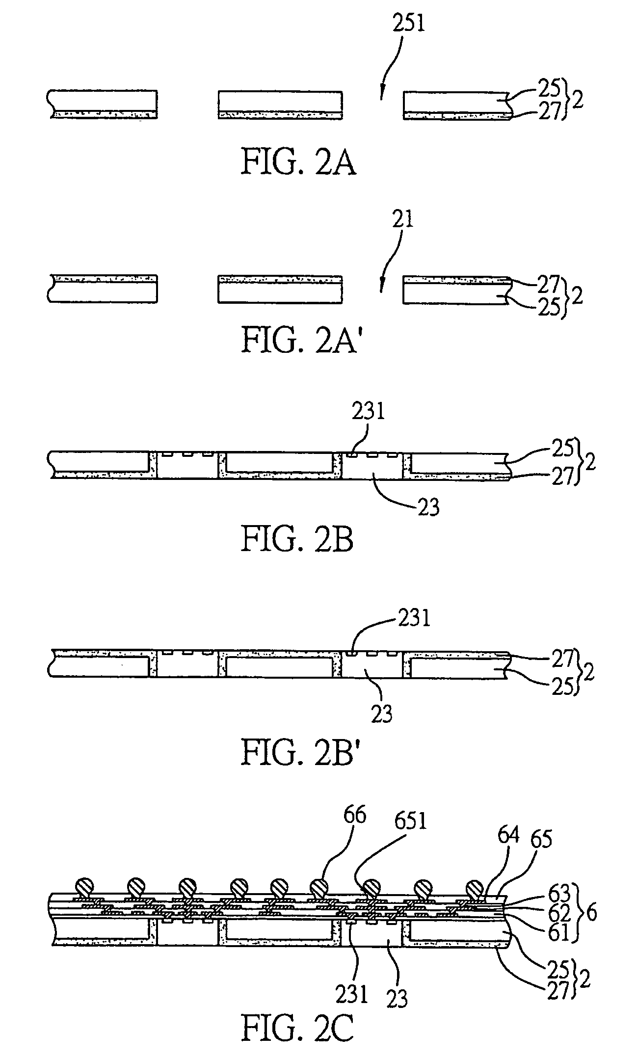
[0024]Referring now to FIGS. 2A and 2B showing schematic diagrams of the carrying structure of electronic components of the present invention. The carrying structure 2 comprises a supporting board 25 having at least one cavity 251, wherein an adhesive layer 27 is formed on a surface of the supporting board 25. In this embodiment, the carrying structure 2 may be for example a double-layered structure comprising the supporting board 25 and the adhesive layer 27 formed on the surface of the s...

second embodiment

[0028]The carrying structure of electronic components of this embodiment comprises at least a first supporting board and a second supporting board having at least one cavity, respectively; at least one adhesive layer formed between the first and the second supporting boards; and at least one electronic component comprising an active and non-active face provided in the corresponding cavities of the first and second supporting boards, wherein a portion of the adhesive layer fills a gap between the electronic element and the cavities of the first and second supporting boards, thereby mounting the electronic component in the cavities of the first and second supporting boards.

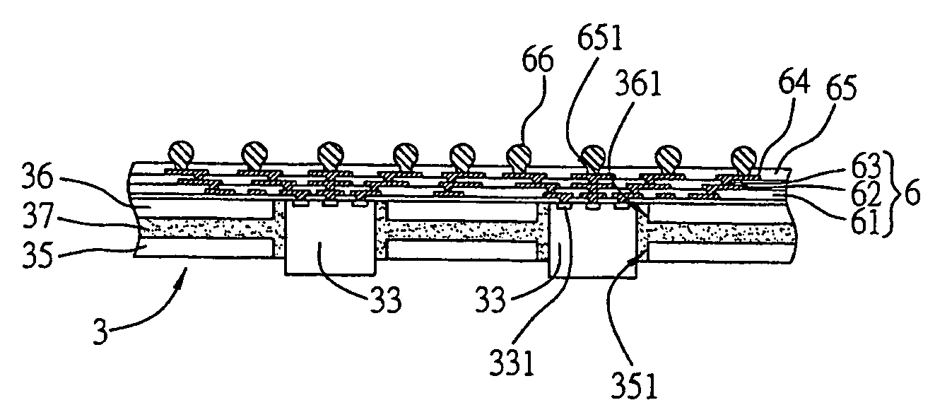
[0029]Referring to FIGS. 3A to 3C, schematic diagrams of a carrying structure 3 for electronic component according to another embodiment of the present invention are shown. The second embodiment essentially differs from the first embodiment in that the carry structure 3 is a multi-layered structure with at least one...

third embodiment

[0034]Referring to FIGS. 4A to 4C, schematic diagrams of a carrying structure of electronic components according to still another embodiment of the present invention are shown, wherein like elements are designated with like reference numerals and will not be described in detail in order to not obscure the features of the present invention.

[0035]As shown in FIG. 4A, the carrying structure comprises a supporting board 25, at least one electronic component 23 and an adhesive layer 27 formed on a surface of the supporting board 25.

[0036]The supporting board 25 has at least one cavity 251. Although the carrying structure 2 is shown as a two-layered structure comprising the supporting board 25 and the adhesive layer 27, however the present invention is not limited to this.

[0037]The electronic component 23 has an active face and a non-active face, where the active face is on the top surface and the non-active face is on bottom surface. The electronic component 23 is disposed in the cavity ...


PUM


Abstract

A carrying structure of electronic components is proposed. The carrying structure includes at least one supporting board with at least one cavity disposed thereon, at least one adhesive layer formed on the supporting board, and at least one electronic component having an active face and a non-active face located in the cavity. The gap between the cavity and the electronic component is filled with a portion of the adhesive layer, and thus the electronic component is fixed in the cavity of the supporting board.

Description

FIELD OF THE INVENTION[0001]The present invention relates to a carrying structure of electronic components, and more particularly, to a carrying structure for carrying and fixing electronic components.BACKGROUND OF THE INVENTION[0002]IBM corp. introduced flip chip package technique in early 1960, the flip chip technique differs from the earlier wire bonding technique in that electrical connections between a semiconductor chip and a circuit board are established through solder bumps rather than traditional gold wires. Advantages of the flip chip technique are increased packaging density and reduced package size. Additionally, the flip chip technique requires no metal conductive wires, thus enhancing electrical properties and satisfying the needs for high-density and high-speed semiconductor devices.[0003]In current flip chip technique, electrode pads are disposed on an active face of a semiconductor IC chip, and corresponding electrode pads are also provided on the circuit board for ...

Claims


Application Information

Patent Timeline
Patent Type & Authority Patents(United States)
IPC IPC(8): H01L21/44
CPCH01L23/5389H01L24/96H01L24/29H01L24/19H01L24/83H01L2224/0401H01L2224/04105H01L2224/16225H01L2224/20H01L2224/83101H01L2224/83192H01L2224/8385H01L2924/01005H01L2924/01012H01L2924/01013H01L2924/01029H01L2924/01056H01L2924/01079H01L2924/01082H01L2924/07802H01L2924/14H01L2924/15174H01L2924/15311H01L2924/18162H01L2924/19041H01L2924/19042H01L2924/19043H01L2924/01006H01L2924/01033H01L2924/014H01L2924/00H01L2224/12105H05K3/42H05K3/40H05K3/46
Inventor HSU, SHIH-PING
Owner PHOENIX PRECISION TECH CORP
Why Eureka
Try Eureka