

Level shifting input buffer circuit
a buffer circuit and input circuit technology, applied in logic circuits, pulse automatic control, pulse technique, etc., can solve the problems of high voltage p-channel transistors in cmos circuits that can be particularly undesirable, undesirably high power consumption, and transistors occupying more spa
- Summary
- Abstract
- Description
- Claims
- Application Information
AI Technical Summary
Benefits of technology
Problems solved by technology
Method used
Image

Examples
Embodiment Construction
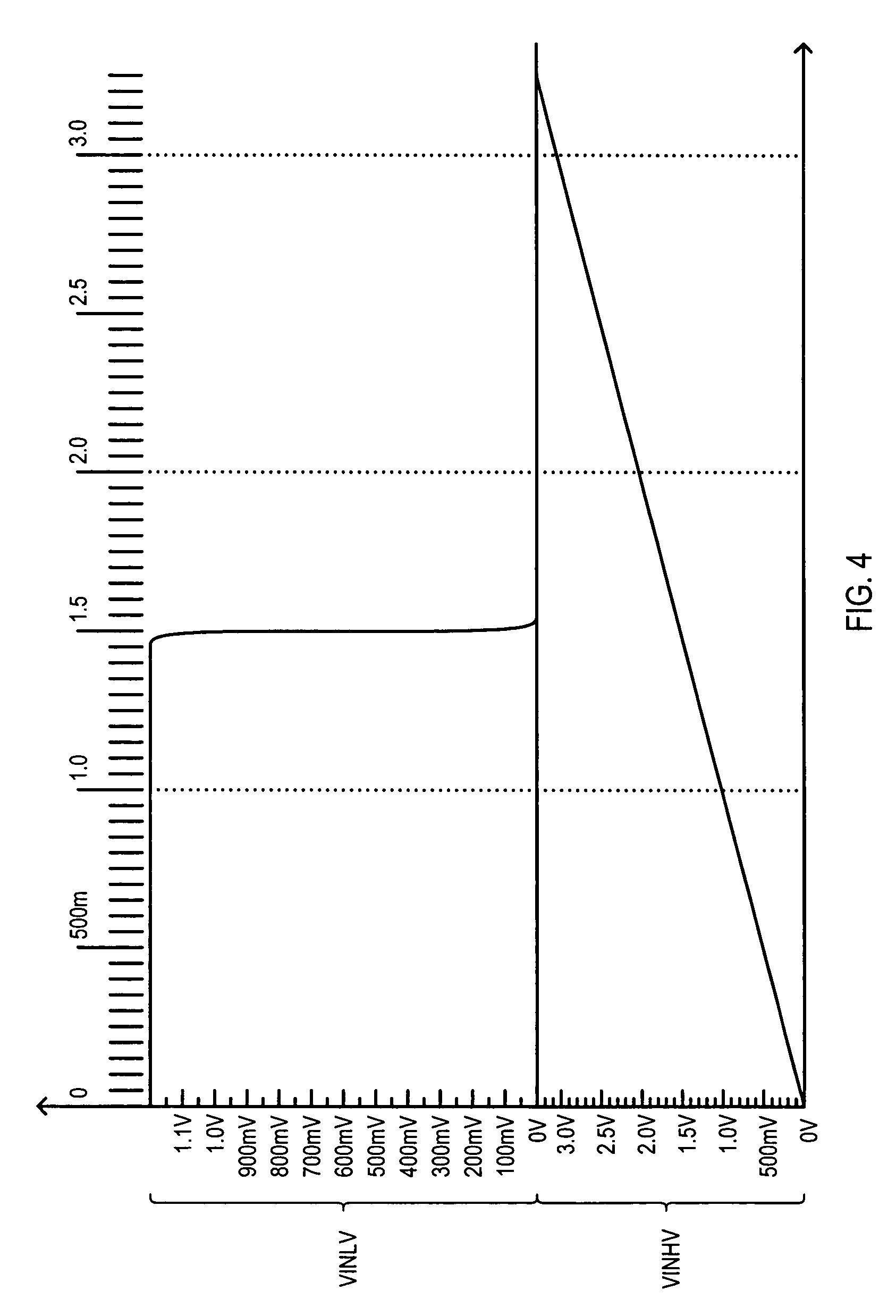
[0052]Various embodiments of the present invention will now be described in detail with reference to a number of drawings. The embodiments include an input circuit that can translate high voltage signals into lower voltage signals. Such an input circuit can be a low voltage circuit, and not require a high voltage power supply.
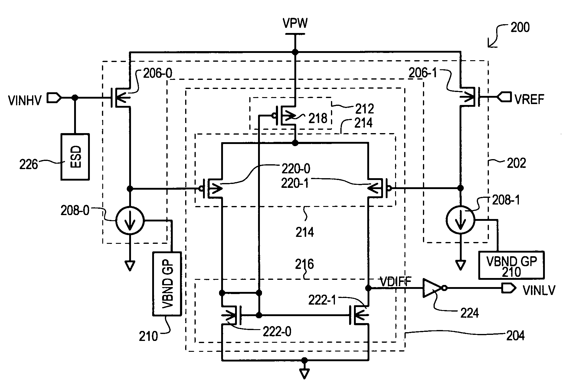
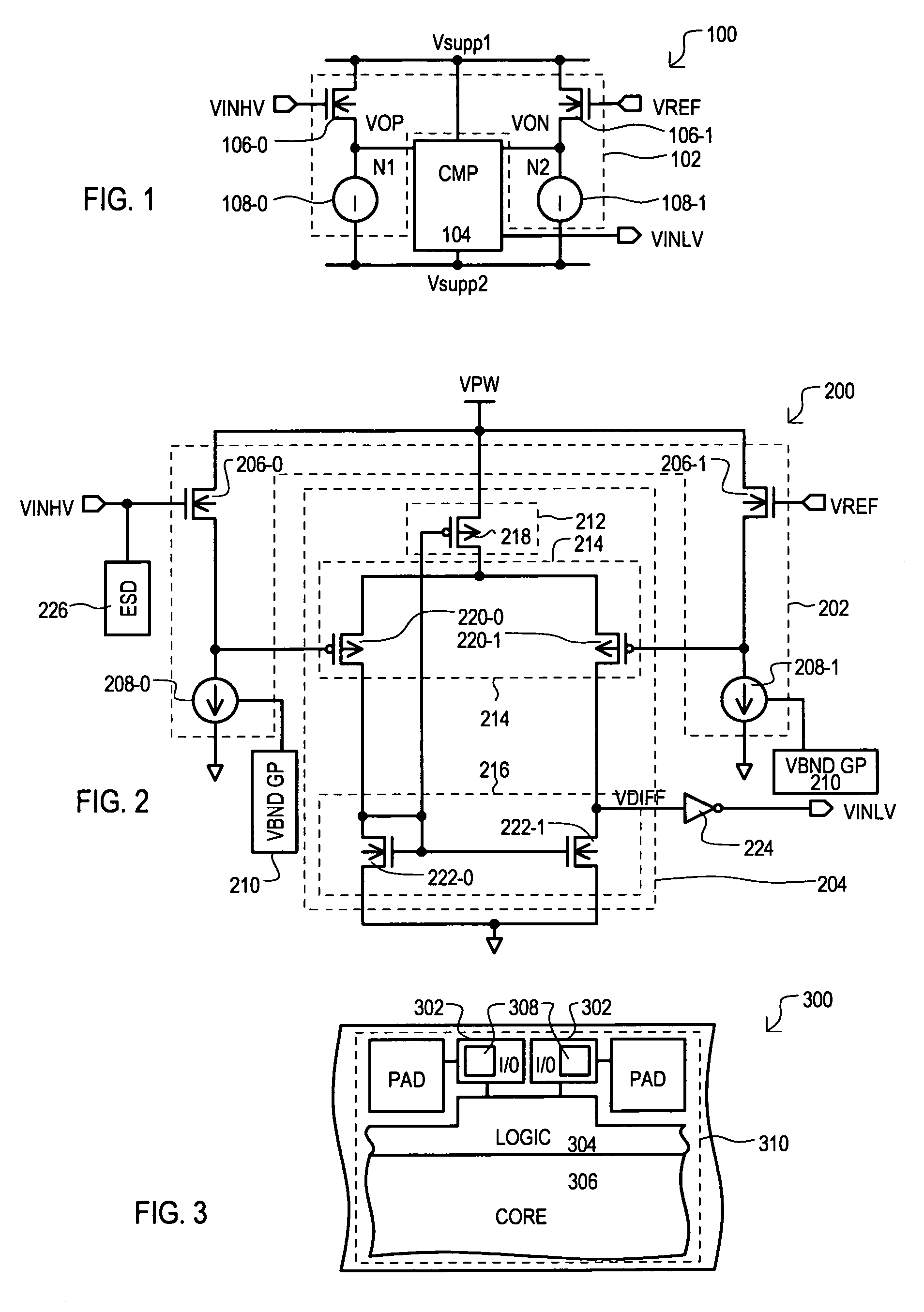
[0053]Referring now to FIG. 1, an input circuit according to one embodiment is shown in a block schematic diagram and designated by the general reference character 100. An input circuit 100 can include a level shifting input section 102 and a compare section 104.
[0054]A level shifting input section 102 can include a first input transistor 106-0, second input transistor 106-1, first current source circuit 108-0 and a second current source circuit 108-1. A first input transistor 106-0 can have a source follower configuration, including a drain connected to a first power supply voltage Vsupp1, a gate that receives a high voltage input signal VINHV, and a source th...
PUM
 Abstract
Description
Claims
Application Information