Active optical alignment using MEMS mirrors

Active Publication Date: 2007-10-02
LUCENT TECH INC +1
View PDF12 Cites 19 Cited by
  • Summary
  • Abstract
  • Description
  • Claims
  • Application Information

AI Technical Summary

Benefits of technology

[0005]In accordance with the present invention, one or more MEMS mirrors is disposed in an optical package and positioned to reflect optical signals between an active optical device (e.g., one or more sources / detectors) located in the package and a passive receiver of light (e.g., transmission fiber, optical waveguide) located at a communication port on a package wall. In operation, the active optical device is turned on and the optical coupling between the active device and the passive device is measured. The deflection profile of the MEMS mirror(s) is then adjusted, using an electrical input signal, until maximum coupling is achieved. The use of a MEMS mirror to “fine tune” the coupling between the active and passive devices thus eliminates the need to perform the rigorous mechanical alignment (such as using an x-y alignment table) so prevalent in the prior art.

Problems solved by technology

A fundamental problem in making a photonics package such as a laser source module is the alignment of a device such as a laser source module with an optical waveguide.
Conventional packages for photonics arrangements are typically made out of variety of dissimilar materials, such as metal, glass and ceramic, and involve relatively complicated manipulation of components during assembly.
These alignment steps depend upon fairly specialized, expensive equipment.

Method used


Image

  • Active optical alignment using MEMS mirrors
  • Active optical alignment using MEMS mirrors
  • Active optical alignment using MEMS mirrors

Examples


Embodiment Construction

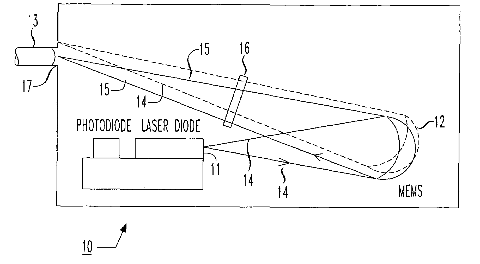
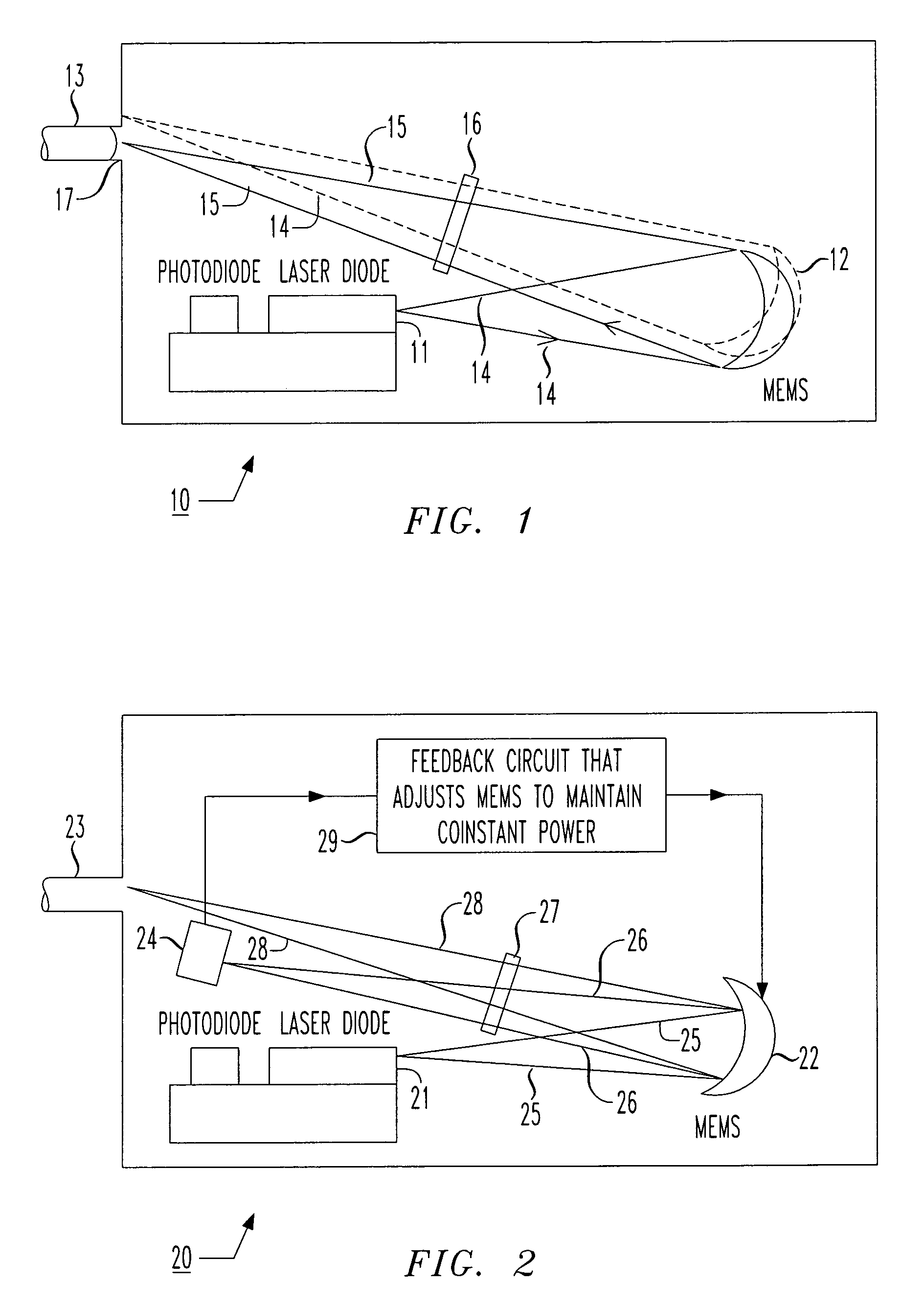
[0015]The present invention will best be understood from the detailed description given below, as well as from the accompanying drawings of the embodiments of the present invention which, however, should not be taken to limit the invention to specific embodiments, but rather are for explanation and understanding only.

[0016]Referring to FIG. 1, there is shown one embodiment of the invention. In particular, FIG. 1 shows a basic package embodiment of the invention that couples light from a light source to an optical fiber output (or another passive output device, such as an optical waveguide) that is attached to an outside wall of the package. As shown, package 10 includes a laser diode light source 11, a MEMS mirror 12 and a fiber 13. Laser diode 11 generates a conical-shaped beam of light 14 which propagates toward MEMS mirror 12. As mentioned above and will be discussed in detail below, the deflection profile of MEMS mirror 12 is electrically adjusted (through a well-known process) ...


PUM


Abstract

An optical package includes one or more MEMS mirrors to provide alignment between internal optical components and the signal port(s) on the package (where one or more ports may include optical fiber attachments). Once the components are placed in the package, an electrical signal is used to adjust the deflection profile of the appropriately positioned MEMS mirror(s) until maximum coupling between the internal components and the fibers / ports is obtained. Advantageously, if later signal degradation occurs due to, for example, subsequent physical misalignment of the internal components, corrective electrical signal can be sent to the MEMS mirror(s) to provide correction and re-alignment without having to open the package and physically move the components.

Description

CROSS-REFERENCE TO RELATED APPLICATION[0001]The present application claims the benefit of Application Ser. No. 60 / 436,434, filed Dec. 24, 2002.BACKGROUND OF THE INVENTION[0002]One of the major advances in recent years has been the increased use of optical communication systems for carrying very large quantities of information with low distortion and at a relatively low cost over great distances. Optical systems are also promising for such purposes as computing because of the inherently high speeds at which they can be operated. For these reasons, considerable development work ha been done in making various photonics packages for use in such systems. Photonics generally refers to devices that share both electronic and optical attributes, such as lasers, which generate coherent light in response to an electrical signal, and photodetectors, which generate an electrical signal in response to light.[0003]A fundamental problem in making a photonics package such as a laser source module is...

Claims


Application Information

Patent Timeline
IPC IPC(8): G01B11/00
CPCG02B6/4225G02B26/0833G02B7/003G02B6/4214G02B6/4246
Inventor BOCK, TIMOTHY PAULOSENBACH, JOHN WILLIAMSCHLENKER, RORY KEENE
Owner LUCENT TECH INC
Why Eureka
Try Eureka