

Testing assembly for electrical test of electronic package and testing socket thereof
a technology of testing assembly and electronic package, which is applied in the direction of electrical testing, measurement devices, instruments, etc., can solve the problems of reducing the return loss of signal transmission, deteriorating the testing accuracy of testing assembly, and impedance mismatch in the entire signal transmission path, so as to improve the impedance continuity of the signal transmission path
- Summary
- Abstract
- Description
- Claims
- Application Information
AI Technical Summary
Benefits of technology
Problems solved by technology
Method used
Image

Examples
Embodiment Construction
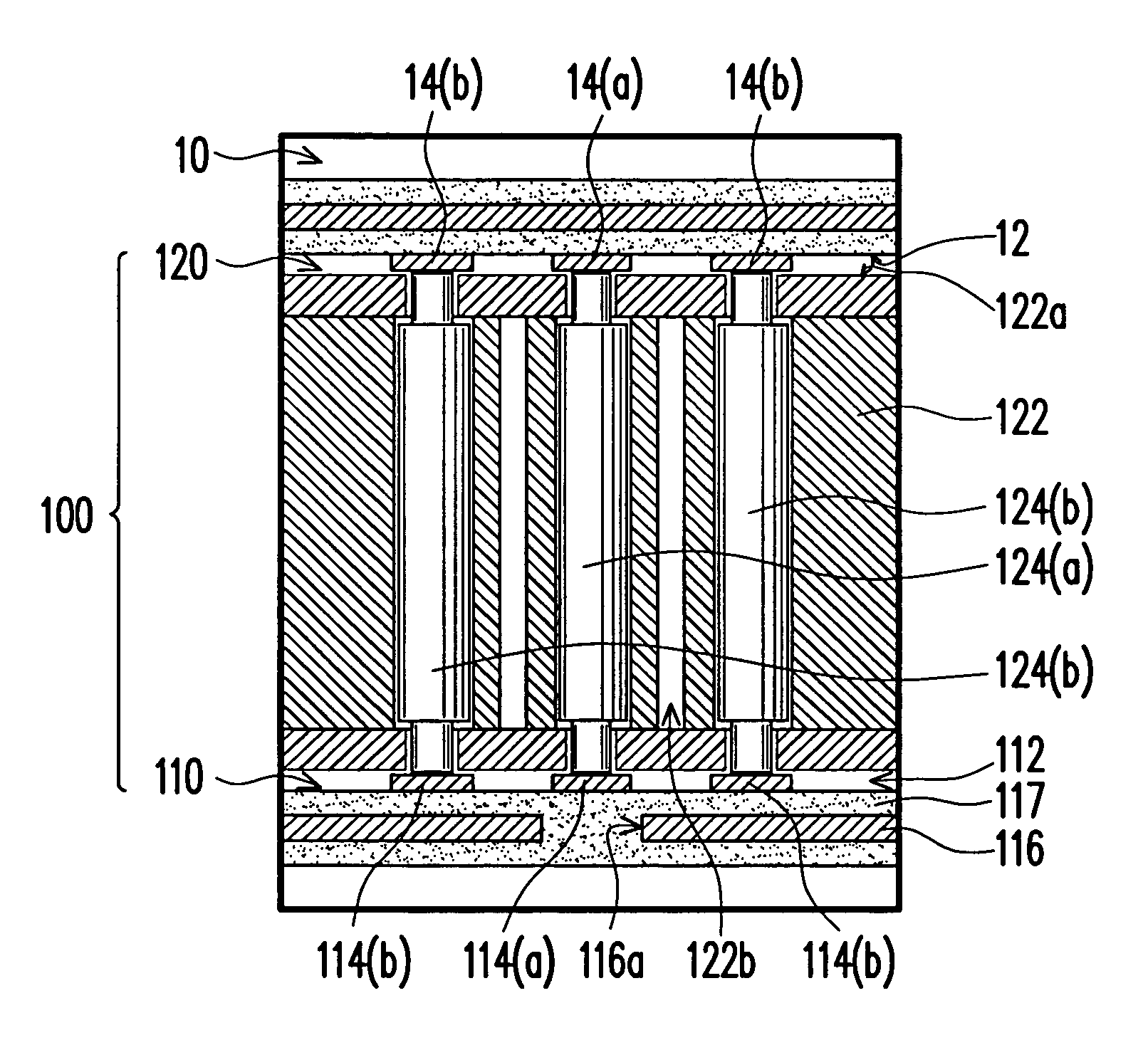
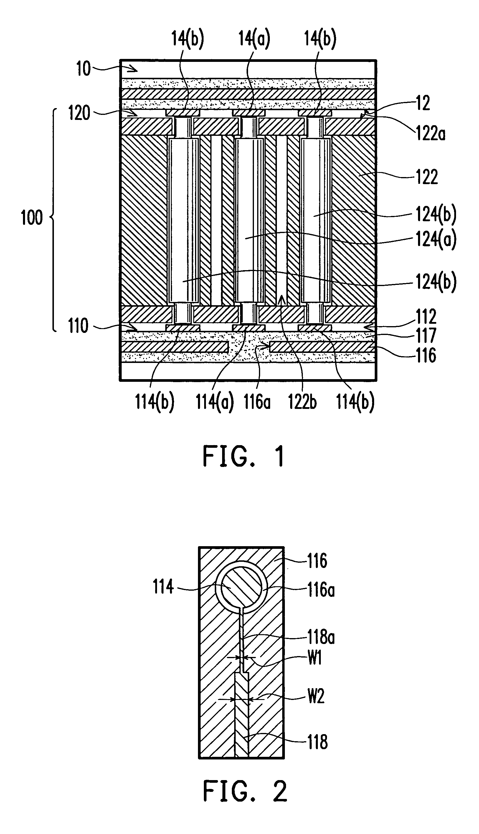
[0019]FIG. 1 is a partial vertical cross-sectional view of a testing assembly according to a first embodiment of the present invention. A testing assembly 100 of a first embodiment of the present invention is suitable for the electrical test of an area array contact package 10, such as a Land Grid Array (LGA) package, a Ball Grid Array (BGA) package, or a Pin Grid Array (PGA) package, and it is also suitable for the electrical test of the peripheral contact package 10, such as a Quad Flat No-lead (QFN) package. In the first embodiment, the package 10 is a LGA type package for example, and only a portion of the package substrate of the package 10 is used herein to represent the package 10. In addition, the package 10 has a plurality of contacts 14, and the contacts 14 are disposed on a contact surface 12 of the package 10.
[0020]The testing assembly 100 of the first embodiment comprises a testing circuit board 110 and a testing socket 120. The testing socket 120 is mounted on the test...
PUM
 Abstract
Description
Claims
Application Information