Low-capacitance contact for long gate-length devices with small contacted pitch

a technology of low-capacitance contact and gate-length device, which is applied in the field of field-effect transistors, can solve the problems of limited leakage power in the scaling of cmos transistor gate lengths, and achieve the effects of minimizing leakage power, reducing length, and maximizing transistor density

Inactive Publication Date: 2007-10-16
INT BUSINESS MASCH CORP
View PDF11 Cites 10 Cited by
  • Summary
  • Abstract
  • Description
  • Claims
  • Application Information

AI Technical Summary

Benefits of technology

[0005]In view of the foregoing, embodiments of the invention provide planar and non-planar field effect transistor (FET) structures and methods of forming the structures. The structures comprise segmented active devices (e.g., multiple semiconductor fins for a non-planar transistor or multiple semiconductor layer sections for a planar transistor) connected at opposite ends to source / drain bridges. A gate electrode is patterned on the segmented active devices between the source / drain bridges such that it has a reduced length between the segments (i.e., between the semiconductor fins or sections). Source / drain contacts land on the source / drain bridges such that they are opposite only those portions of the gate electrode with the reduced gate length. These FET structures can be configured to simultaneously maximize the density of the transistor, minimize leakage power and maintain the parasitic capacitance between the source / drain contacts and the gate conductor below a preset level, depending upon the performance and density requirements.
[0008]A plurality of source / drain contacts can connect to the second sections. The contacts can be positioned above the second sections between the first sections such that they are opposite the second (shorter) portions of the gate conductor. The different lengths of the gate conductor and a pitch between the contacts can be predetermined based on performance and density requirements for the transistor so as to simultaneously maximize the density the transistor, minimize leakage power and maintain parasitic capacitance below a preset level.
[0012]A plurality of source / drain contacts can connect to the semiconductor mesas. The contacts can be positioned above the semiconductor mesas between the semiconductor fins such that they are opposite the second (shorter) portions of the gate conductor. As with the previously described planar embodiment, the different lengths of the gate conductor and a pitch between the contacts are predetermined based on performance and density requirements for the transistor in order to simultaneously maximize the density of transistor, minimize leakage power and maintain parasitic capacitance below a preset level.
[0016]In order to simultaneously maximize the density of the resulting transistor, minimize leakage power and maintain parasitic capacitance below a preset level, the different lengths of the gate conductor and a pitch between the contacts can be predetermined (e.g., during the design phase before forming the semiconductor layer) based on performance and density requirements.
[0021]In order to simultaneously maximize the density of the resulting transistor, minimize leakage power and maintain parasitic capacitance below a preset level, the different lengths of the gate conductor and a pitch between the contacts can be predetermined (e.g., during the design phase before forming of the semiconductor bodies) based on performance and density requirements for the transistor.

Problems solved by technology

Despite current lithography techniques which allow devices to be formed with reduced dimensions, the scaling of complementary metal oxide semiconductor (CMOS) devices and particularly, the scaling of CMOS transistor gate lengths is limited by leakage power.

Method used


Image

  • Low-capacitance contact for long gate-length devices with small contacted pitch
  • Low-capacitance contact for long gate-length devices with small contacted pitch
  • Low-capacitance contact for long gate-length devices with small contacted pitch

Examples


Embodiment Construction

[0035]The embodiments of the invention and the various features and advantageous details thereof are explained more fully with reference to the non-limiting embodiments that are illustrated in the accompanying drawings and detailed in the following description. It should be noted that the features illustrated in the drawings are not necessarily drawn to scale. Descriptions of well-known components and processing techniques are omitted so as to not unnecessarily obscure the embodiments of the invention. The examples used herein are intended merely to facilitate an understanding of ways in which the embodiments of the invention may be practiced and to further enable those of skill in the art to practice the embodiments of the invention. Accordingly, the examples should not be construed as limiting the scope of the embodiments of the invention.

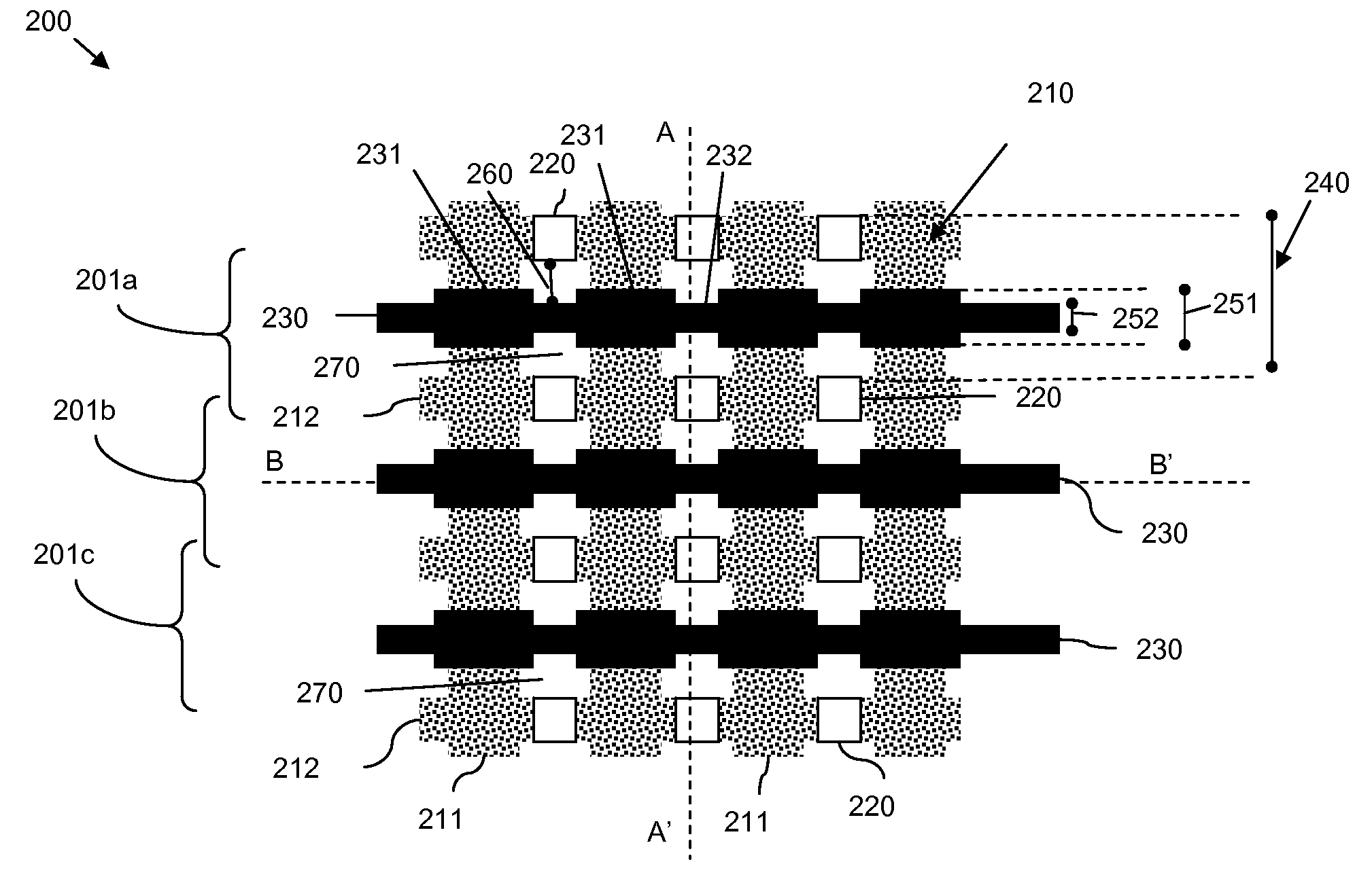
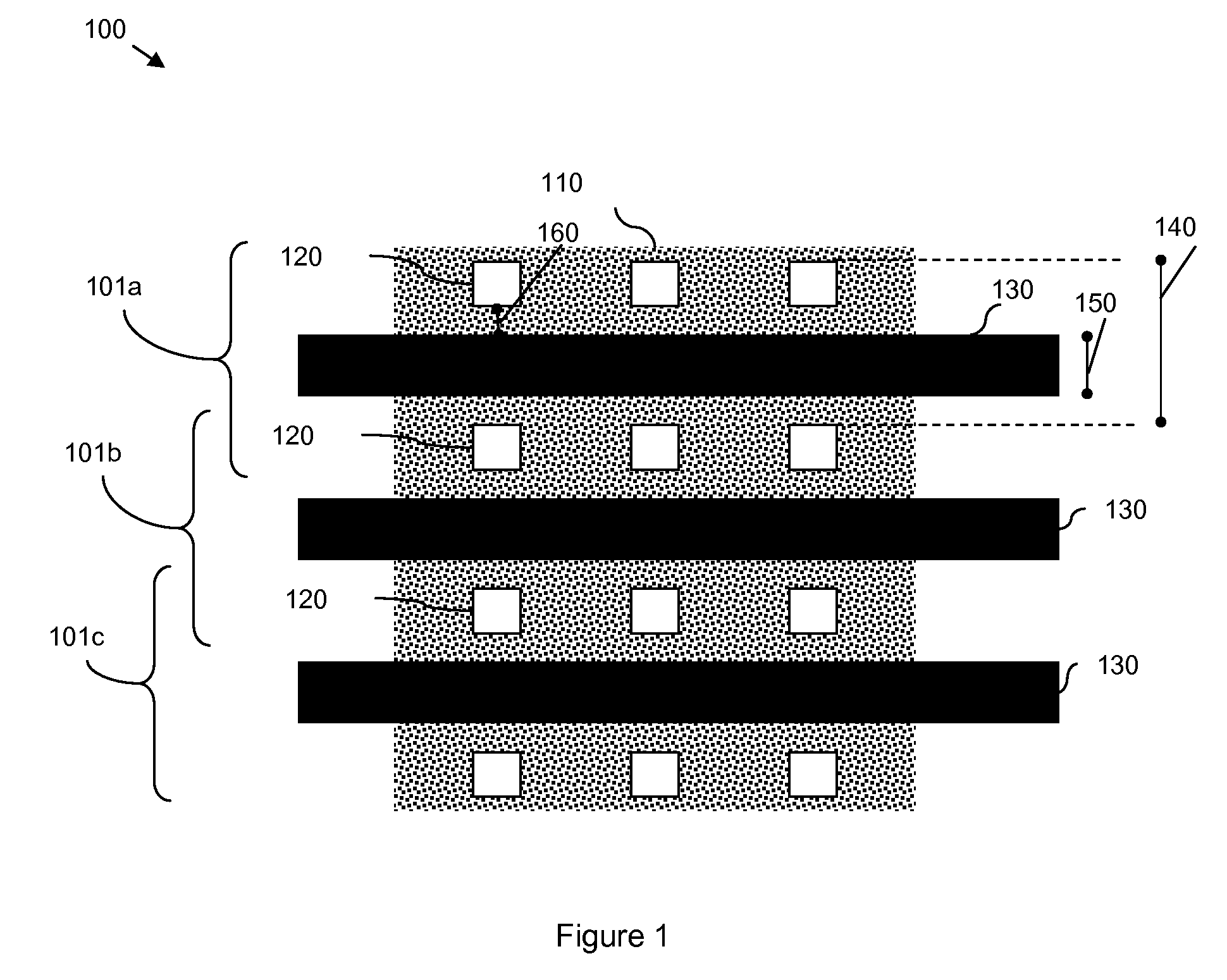
[0036]FIG. 1 illustrates semiconductor structure 100 comprising multiple planar field effect transistors 101a-c. More specifically, the structur...


PUM


Abstract

Disclosed are planar and non-planar field effect transistor (FET) structures and methods of forming the structures. The structures comprise segmented active devices (e.g., multiple semiconductor fins for a non-planar transistor or multiple semiconductor layer sections for a planar transistor) connected at opposite ends to source / drain bridges. A gate electrode is patterned on the segmented active devices between the source / drain bridges such that it has a reduced length between the segments (i.e., between the semiconductor fins or sections). Source / drain contacts land on the source / drain bridges such that they are opposite only those portions of the gate electrode with the reduced gate length. These FET structures can be configured to simultaneously maximize the density of the transistor, minimize leakage power and maintain the parasitic capacitance between the source / drain contacts and the gate conductor below a preset level, depending upon the performance and density requirements.

Description

BACKGROUND[0001]1. Field of the Invention[0002]The embodiments of the invention generally relate to field effect transistors, and, more particularly, to a low-capacitance contact for long gate-length planar and non-planar devices with small contacted pitch.[0003]2. Description of the Related Art[0004]Despite current lithography techniques which allow devices to be formed with reduced dimensions, the scaling of complementary metal oxide semiconductor (CMOS) devices and particularly, the scaling of CMOS transistor gate lengths is limited by leakage power. Logic circuit density is limited by the contacted pitch of field effect transistors (i.e., the minimum metal line width spacing plus addition for via or contact covers or landing pads) and this contacted pitch is in turn limited by the (non-shrinking) gate lengths of the transistors. It would be advantageous over the prior art to provide a transistor structure that can simultaneously minimize leakage power, minimize parasitic capacit...

Claims


Application Information

Patent Timeline
Patent Type & Authority Patents(United States)
IPC IPC(8): H01L29/76
CPCH01L21/823431H01L21/823456H01L27/088H01L27/0886H01L29/41791H01L29/66795H01L29/785H01L27/1211H01L2029/7858
Inventor ANDERSON, BRENT A.NOWAK, EDWARD J.
Owner INT BUSINESS MASCH CORP
Why Eureka
Try Eureka