Frequency characteristics-variable amplifying circuit and semiconductor integrated circuit device

Inactive Publication Date: 2007-10-16
RENESAS ELECTRONICS CORP
View PDF8 Cites 8 Cited by
  • Summary
  • Abstract
  • Description
  • Claims
  • Application Information

AI Technical Summary

Benefits of technology

[0018]A semiconductor integrated circuit device according to the present invention has the above-described frequency characteristics-variable amplifying circuit. In the present invention, by mounting the above-described frequency characteristics-variable amplifying circuit on a semiconductor integrated circuit device together with a gain-variable amplifying circuit, etc., a broadband amplifier which can vary frequency characteristics of output signals can be manufactured.
[0019]According to the present invention, by providing a variable capacitor in a frequency characteristics-variable amplifying circuit and changing a control voltage to be applied to this variable capacitor, a load impedance inside the above-described frequency characteristics-variable amplifying circuit can be changed. Thereby, since frequency characteristics of inputted signals are changed, even when various signals are inputted, the waveform of output signals can be rectified.

Problems solved by technology

However, since the prior-art amplifying circuit 50 cannot vary frequency characteristics of inputted signals, the amplifying circuit cannot control the peaking position and cannot correspond to frequencies other than a frequency presumed in design, therein exists a problem.

Method used


Image

  • Frequency characteristics-variable amplifying circuit and semiconductor integrated circuit device
  • Frequency characteristics-variable amplifying circuit and semiconductor integrated circuit device
  • Frequency characteristics-variable amplifying circuit and semiconductor integrated circuit device

Examples


Embodiment Construction

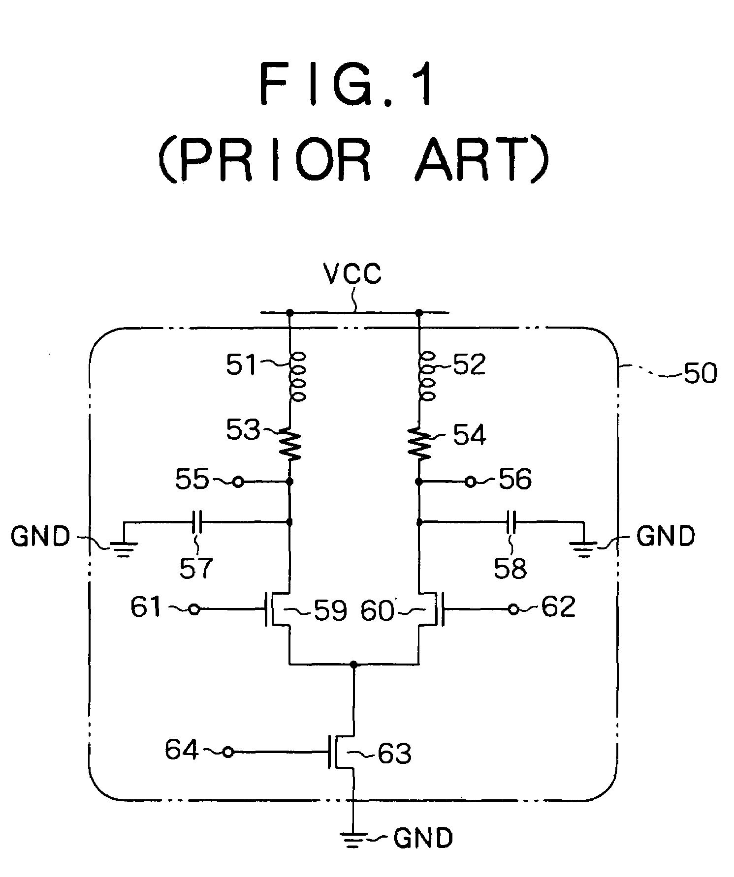
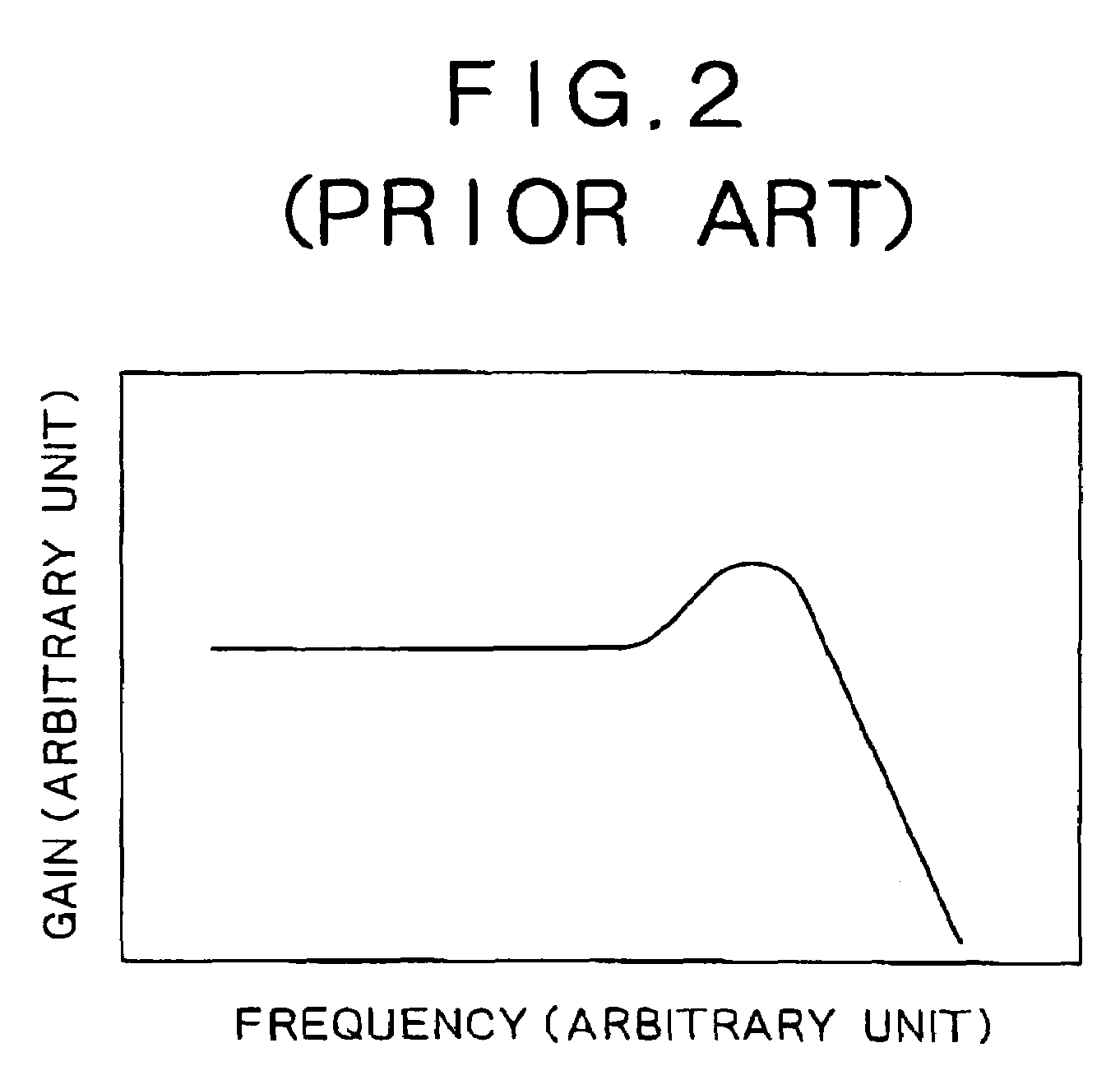
[0026]Hereinafter, a frequency characteristics-variable amplifying circuit according to the embodiment of the present invention will be described in detail with reference to the attached drawings. FIG. 3 is a circuit diagram showing the frequency characteristics-variable amplifying circuit according to the embodiment of the present invention. As shown in FIG. 3, a frequency characteristics-variable amplifying circuit 1 of the present embodiment is connected between power supply potential wiring and ground potential wiring. This frequency characteristics-variable amplifying circuit 1 is, for example, a part of an integrated circuit formed on a silicon substrate. In the frequency characteristics-variable amplifying circuit 1, from the power supply potential wiring to the ground potential wiring, an inductor 2, a resistor 6, an output terminal 8, and an NMOS transistor 10 are series-connected in this order, and in parallel with these, an inductor 3, a resistor 7, an output terminal 9, ...


PUM


Abstract

From power supply potential wiring to ground potential wiring, a first inductor, a first resistance, a first output terminal, and a first transistor are series-connected in this order, and in parallel with these, a second inductor, a second resistor, a second output terminal, and a second transistor are series-connected in this order. And, one electrode of a first variable capacitor is connected between the first inductor and first resistor, and one electrode of a second variable capacitor is connected between the second inductor and second resistor. The other electrodes of the first variable capacitor and second variable capacitor are connected to a first frequency characteristics control terminal and a second frequency characteristics control terminal, respectively. In addition, drains of the first transistor and second transistors are connected to the first output terminal and second output terminal, respectively, sources of the same are connected to a drain of a third transistor, and gates of the same are connected to a first input terminal and a second input terminal, respectively. Furthermore, a gate of the third transistor is connected to a bias terminal, and a source of the same is connected to the ground potential wiring.

Description

BACKGROUND OF THE INVENTION[0001]1. Field of the Invention[0002]The present invention relates to a frequency characteristics-variable amplifying circuit for amplifying a high-frequency signal and a semiconductor integrated circuit device mounted with this frequency characteristics-variable amplifying circuit.[0003]2. Description of the Related Art[0004]An optical communications receiving module is mounted with a photo-detector to convert a light signal to an electric signal and a broadband amplifier into which an electric signal outputted from this photo-detector is inputted and which rectifies a signal waveform attenuated and distorted during a transmission through an optical fiber. This broadband amplifier is composed of an amplifier mainly for amplifying an attenuated signal and an amplifier for mainly rectifying a waveform disorder. Recently, with the realization of downsized and low-cost optical communications modules, broadband amplifiers wherein the respective amplifiers are ...

Claims


Application Information

Patent Timeline
Patent Type & Authority Patents(United States)
IPC IPC(8): H03F3/45H03F3/04H03F3/193H03H11/04
CPCH03F3/193H03F3/45183H03F2203/45704H03F2203/45638H03F2203/45702H03F2203/45631
Inventor OKAMOTO, FUYUKI
Owner RENESAS ELECTRONICS CORP
Why Eureka
Try Eureka