

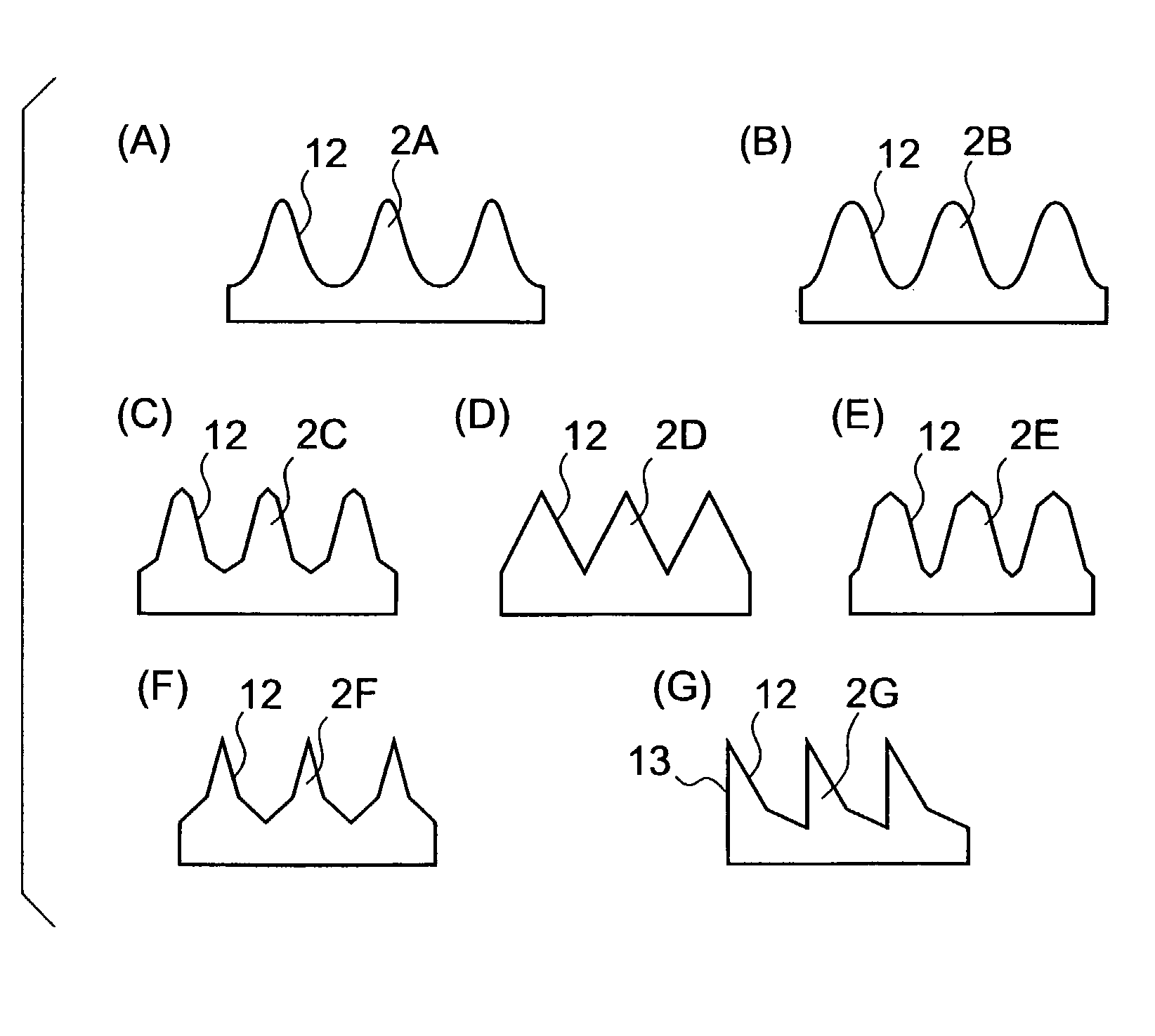
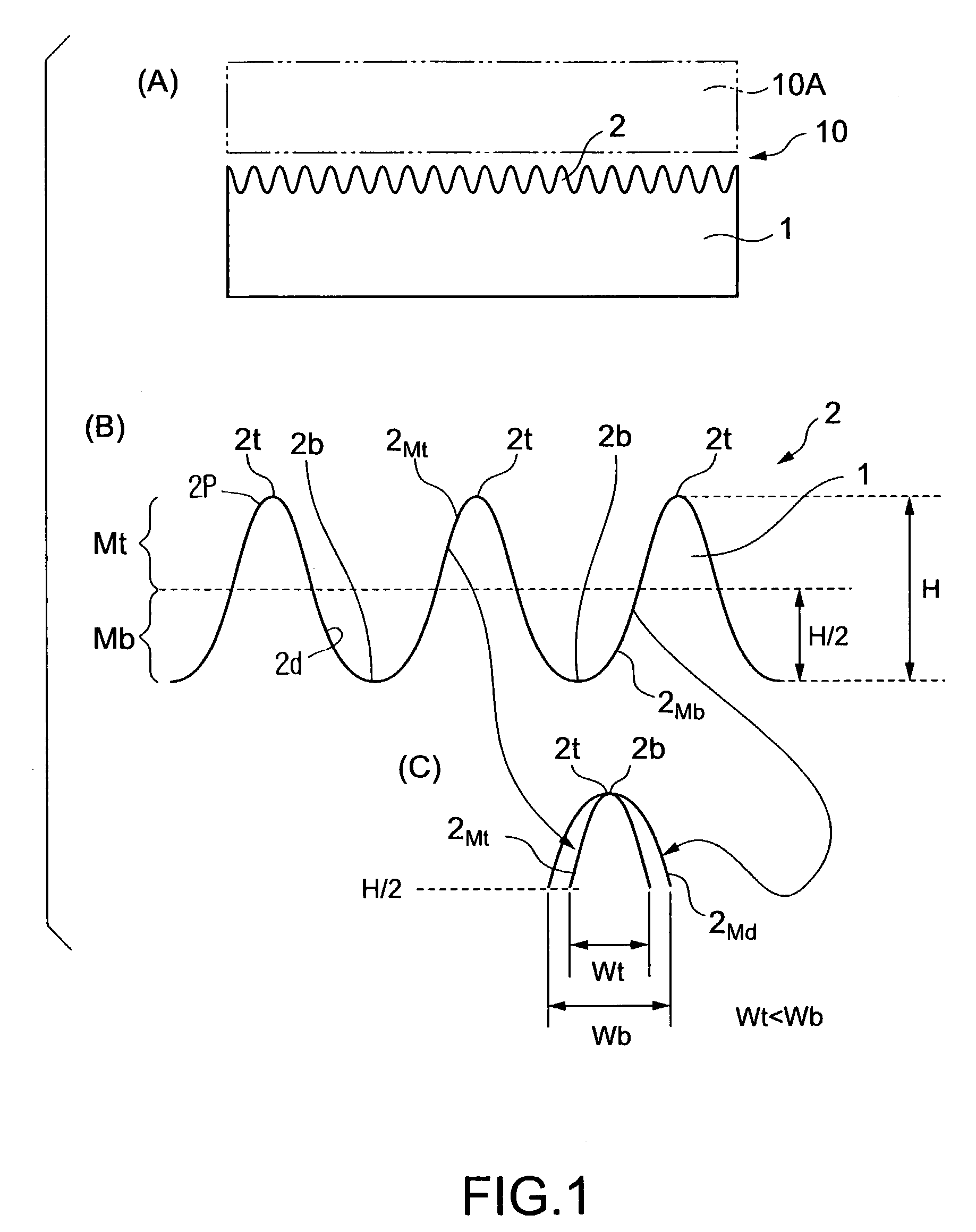
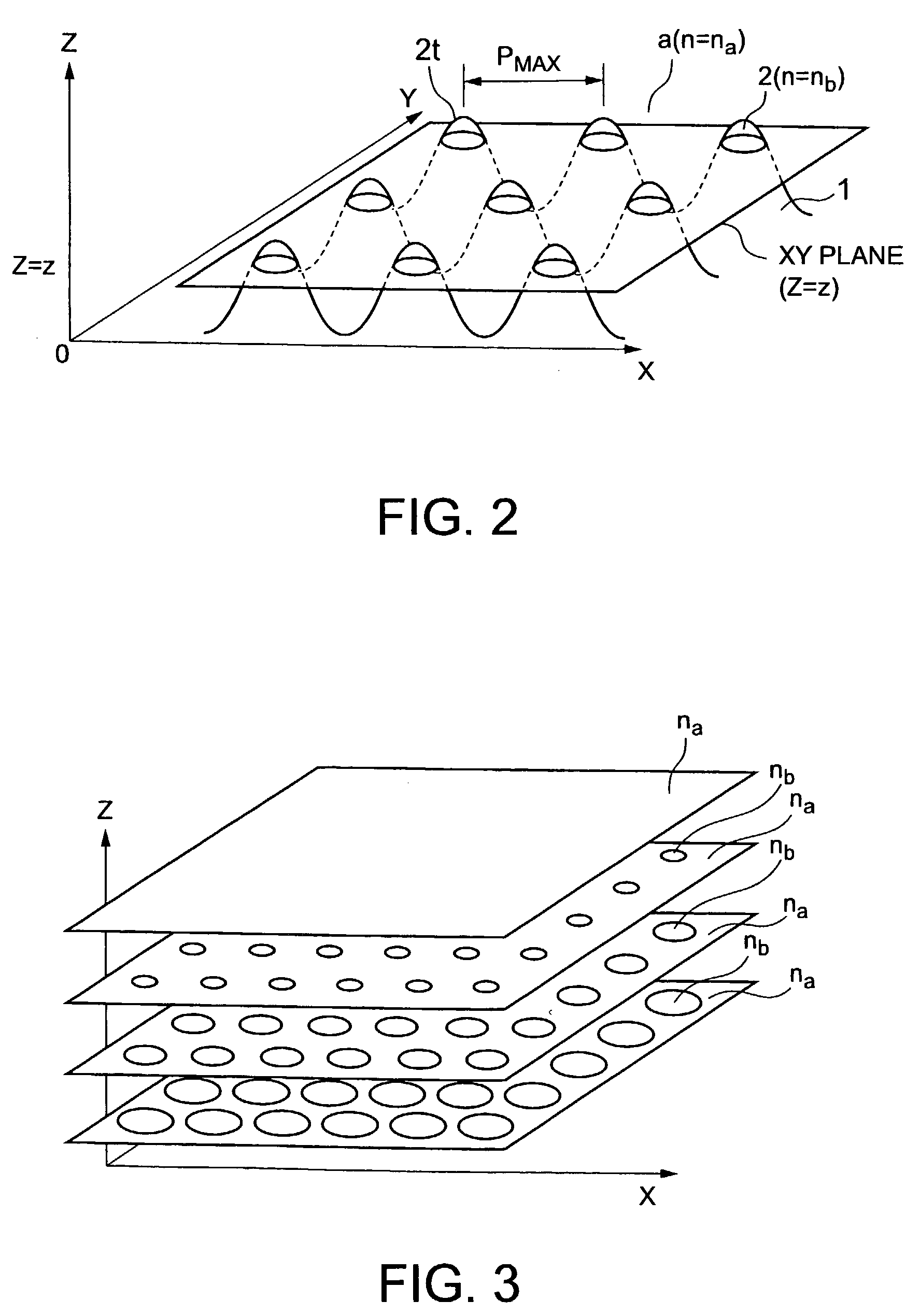
Antireflection structure
a technology of anti-reflection and structure, which is applied in the direction of instruments, other domestic objects, transportation and packaging, etc., can solve the problems of deteriorating deteriorating the visibility of matters displayed on the display panel, and reducing the efficiency of utilization of light emitted by the display panel, so as to prevent reflection and improve the efficiency of display light , the effect of improving the visibility of the screen
- Summary
- Abstract
- Description
- Claims
- Application Information
AI Technical Summary
Benefits of technology
Problems solved by technology
Method used
Image

Examples
example 1
[0136]A base plate for a photomask was formed by forming a chromium film on a surface of a 152.4 mm (6 in.) square 6.35 mm thick synthetic quartz plate. A resist film was formed over the chromium film by spreading a positive EB resist (“ZEP7000”, Nippon Zeon K.K.) by a spin coater. A mesh pattern having longitudinal and transverse pitches of 300 nm was written on the resist film on the basis of mesh pattern data for exposure, the exposed resist film was developed by using a predetermined developer to obtain a resist pattern having open meshes. Then, parts of the chromium film corresponding to the meshes of the resist pattern were etched through the resist pattern by a dry etching process to form openings in the chromium film. The dry etching process used a dry etching system “VERSALOCK7000” commercially available from Unaxis Co.
[0137]Subsequently, the base plate was etched by a dry etching process using the resist pattern and the chromium film as an etching mask, and fluorine gas as...
example 2
[0142]A base plate for a photomask was formed by forming a photoresist film of a photoresist (“S1805”, Sipray Co.) on a surface of a 127 mm (5 in.) square 3 mm thick soda glass plate by a spin coating process. The photoresist film was exposed to laser light emitted by an argon ion laser from two directions at 60° to a plane perpendicular to the surface of the glass plate by exposure energy of 120 mJ. Then, the glass plate was turned through an angle of 90°, and the photoresist film was exposed to laser light under the same exposure conditions. Then, the photoresist film thus exposed was subjected to a developing process using a dilute developer (“Developer CONC”, Sipray Co.) having a concentration of 32% for twenty-five seconds. Thus, a mother plate provided with a desired finely roughened part having projections and depressions, in which tip parts of the projections were sharper than bottom parts of the depressions. A laser exposure system used for exposing the photoresist film to ...
PUM
| Property | Measurement | Unit |
|---|---|---|
| refractive index | aaaaa | aaaaa |
| refractive index na | aaaaa | aaaaa |
| refractive index na | aaaaa | aaaaa |
Abstract
Description
Claims
Application Information