Optically improved CMOS imaging sensor structure to lower imaging lens requirements
a technology of imaging sensor and cmos, which is applied in the field of lowering imaging lens requirements, can solve the problems of requiring a complicated optical design and high manufacturing cost, lens requirements may encounter additional difficulties, and lens thickness requirements may become more significant, so as to reduce the thickness of the sensing portion, the thickness of each layer is reduced, and the lens requirement is low
- Summary
- Abstract
- Description
- Claims
- Application Information
AI Technical Summary
Benefits of technology
Problems solved by technology
Method used
Image
Examples
exemplary embodiment 400
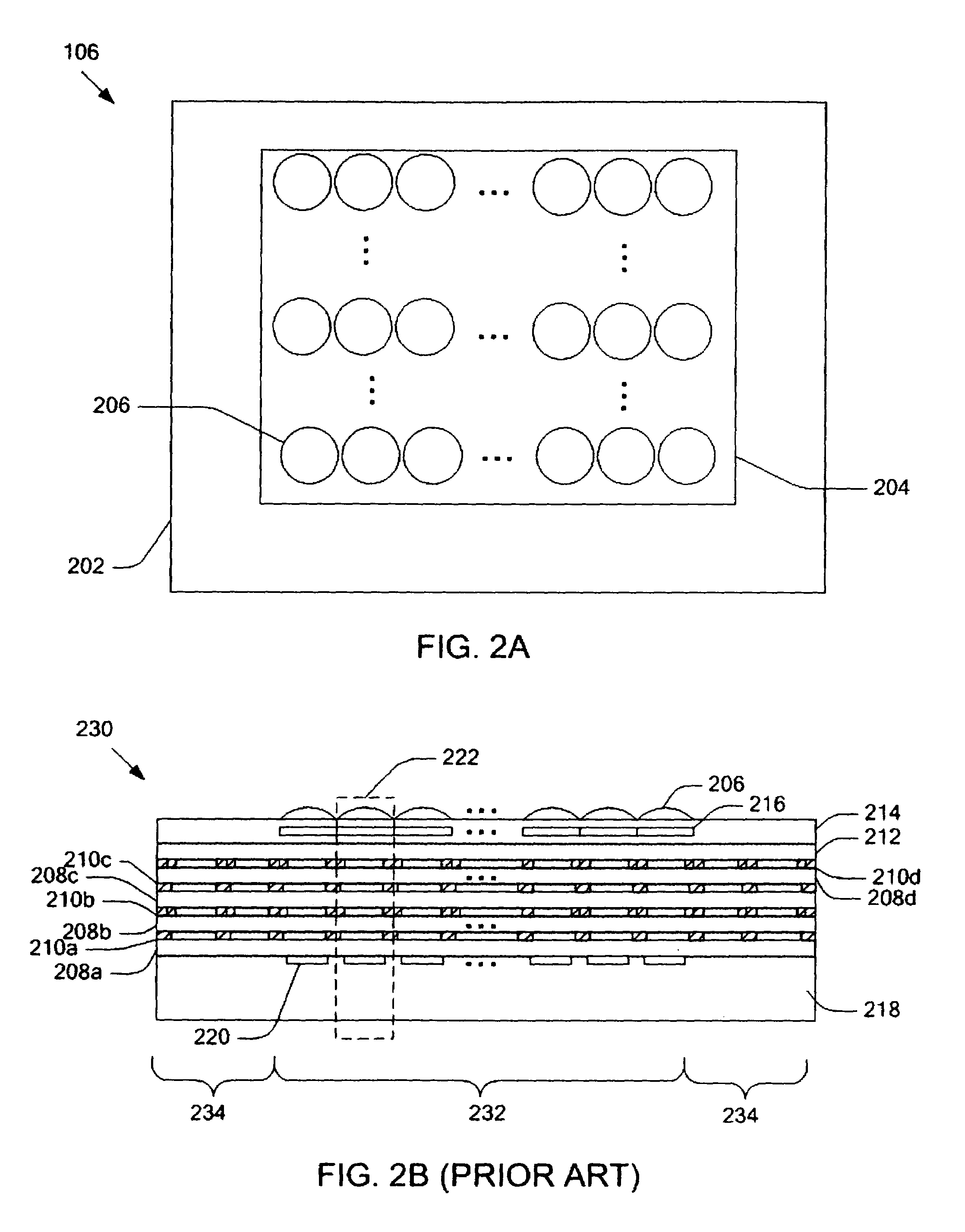
[0035]FIG. 4a is a schematic diagram of an exemplary embodiment 400 of the conventional sensor pixel 222 (shown in FIG. 2b). The sensor pixel 400 may be on a substrate 420 and include: a photodiode 416; four transparent insulating layers 404a-d; four metal layers 406a-d, the four metal layers being insulated by the four transparent insulating layers 404a-d and connected to the photodiode 416; a passivation layer 408, the passivation layer being a transparent insulating layer and having a flat top surface; a color filter 410 for transmitting a specific wavelength or wavelength band of light to the photodiode 416; a planar layer 412 for providing a flat surface; and a microlens 414 for focusing light rays to the photodiode 416. Typically, the thicknesses 418 and 419 may be about 7 and 10 microns, respectively.
exemplary embodiment 420
[0036]FIG. 4b is a schematic diagram of an exemplary embodiment 420 of a sensor pixel in accordance with one embodiment of the present invention. The sensor pixel 420 includes: a photodiode 436; two transparent insulating layers 424a-b; two metal layers 426a-b; a passivation layer 428, the passivation layer being a transparent insulating layer and having a flat top surface; a color filter 430 for transmitting a specific wavelength or wavelength band of light to the photodiode 436; a planar layer 432 for providing a flat surface; and a microlens 434 for focusing light rays to the photodiode 436. The sensor die 420 may be similar to the sensor pixel 400 except a difference that the sensor pixel 420 has a smaller number of metal and insulating layers to reduce its thickness. The thicknesses 438 and 439 may be about, but not limited to, 3 and 5 microns, respectively. In one embodiment, to reduce the thicknesses 438 and 439 further, the thickness of each layer of the pixel 420 may be dec...
exemplary embodiment 500
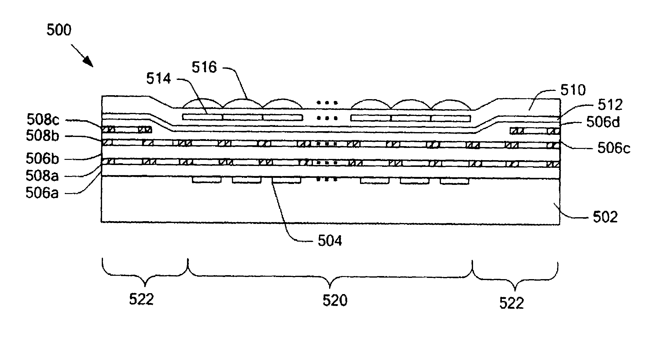
[0037]FIG. 5 is a side cross sectional view of an exemplary embodiment 500 of a sensor die in accordance with one embodiment of the present invention. As illustrated in FIG. 5, the sensing portion 520 of the sensor die 500 may have a smaller number of metal and transparent insulating layers than the non-sensing portion 522. The sensing portion 520 includes: a substrate 502; photodiodes 504; two metal layers 508a-b; three transparent insulating layers 506a-c; a passivation layer 512; a planar layer 510; color filters 514; and microlenses 516. The non-sensing portion 522 may include: the substrate 502; three metal layers 508a-c; four transparent insulating layers 506a-d; the passivation layer 512; and the planar layer 510. In one embodiment, the two insulating layers 506a and 506d may be made of one dielectric material.
[0038]Typically, as illustrated in FIG. 2b, each layer of the conventional sensor die 230 may have a uniform thickness distribution over the portions 232 and 234. Thus,...
PUM
 Abstract
Description
Claims
Application Information


