Non-volatile, resistive memory cell based on metal oxide nanoparticles, process for manufacturing the same and memory cell arrangement of the same

a resistive memory cell and metal oxide nanoparticle technology, applied in material nanotechnology, digital storage, instruments, etc., can solve the problems of switching cycles, inability to realize high storage density, and inability to achieve high storage density, etc., and achieve the effect of convenient manufacturing

Active Publication Date: 2007-11-20
POLARIS INNOVATIONS LTD
View PDF2 Cites 25 Cited by
  • Summary
  • Abstract
  • Description
  • Claims
  • Application Information

AI Technical Summary

Benefits of technology

[0008]Due to the reduction of the switching and storage effect to only a few or even a single nanoparticle, the memory cell according to the present invention attains a significantly higher storage density at lower cost. Thus, it is possible to realize a lower switching power and faster switching times than in the storage technology with conventionally deposited NiO1−x layers.
[0009]The inventive use of metal oxide nanoparticles enables switching between two bistable resistance states in the nanoparticles. Applying a corresponding voltage within a narrow range allows switching between these resistance states. Due to thermal-electronic interaction with trap centers and metal ion diffusion along the nano-crystalline grain boundaries, the state of high conductivity is stabilized. The formation and disruption of the filament region of high conductivity is furthermore coupled to a thermistor effect. This thermistor effect enhances the diffusion process and the charge and discharge processes in the defective states, due to an inhomogeneous temperature distribution in the metal oxide storage material when applying a voltage.
[0012]Due to the smaller dimensions of the metal oxide nanoparticles and the density and homogeneity of the deposition, memory cells with higher density and improved switching and storage properties can be realized. Therein, it is possible to perform bistable switching with only a single particle of about 3 nm×3-5 nm. Thus, the conductive filament can be reduced in the on-state to dimensions below 3 nm. This size corresponds to the limit for thermo-electronic switching and storage effects.

Problems solved by technology

However, with conventional methods for manufacturing resistively switching metal oxide storage materials, active memory cells of few nanometers in dimension are unattainable.
In addition, this stress may be increased by inhomogeneous heating of a larger layer volume due to the thermistor effect, so that the adhesiveness of the layers often limits the switching cycles, and the layers may peel off (S. Seo, M. J. Lee, D. H. Seo, E. J. Jeoung, D.-S.
Furthermore, a high storage density cannot be realized with this technology, since a reduction in size is difficult.
This severely limits the lifetime.

Method used


Image

  • Non-volatile, resistive memory cell based on metal oxide nanoparticles, process for manufacturing the same and memory cell arrangement of the same
  • Non-volatile, resistive memory cell based on metal oxide nanoparticles, process for manufacturing the same and memory cell arrangement of the same
  • Non-volatile, resistive memory cell based on metal oxide nanoparticles, process for manufacturing the same and memory cell arrangement of the same

Examples


Embodiment Construction

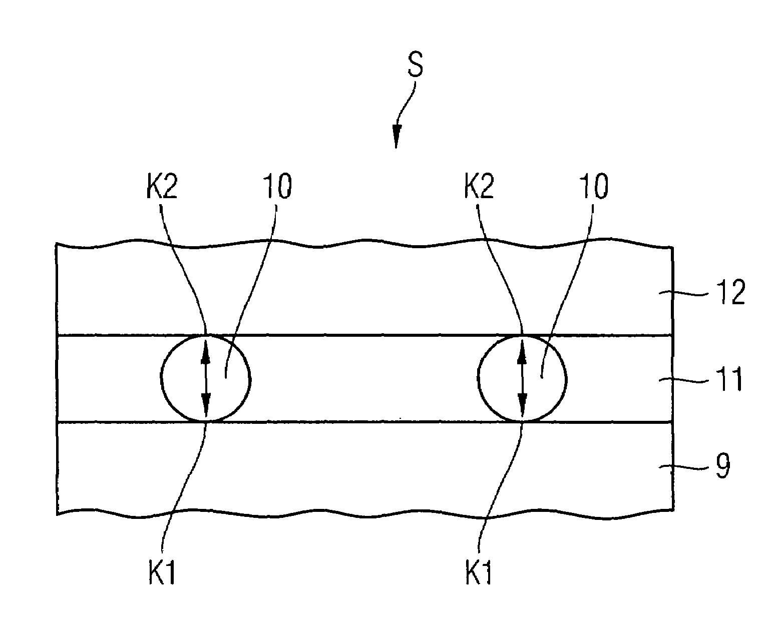
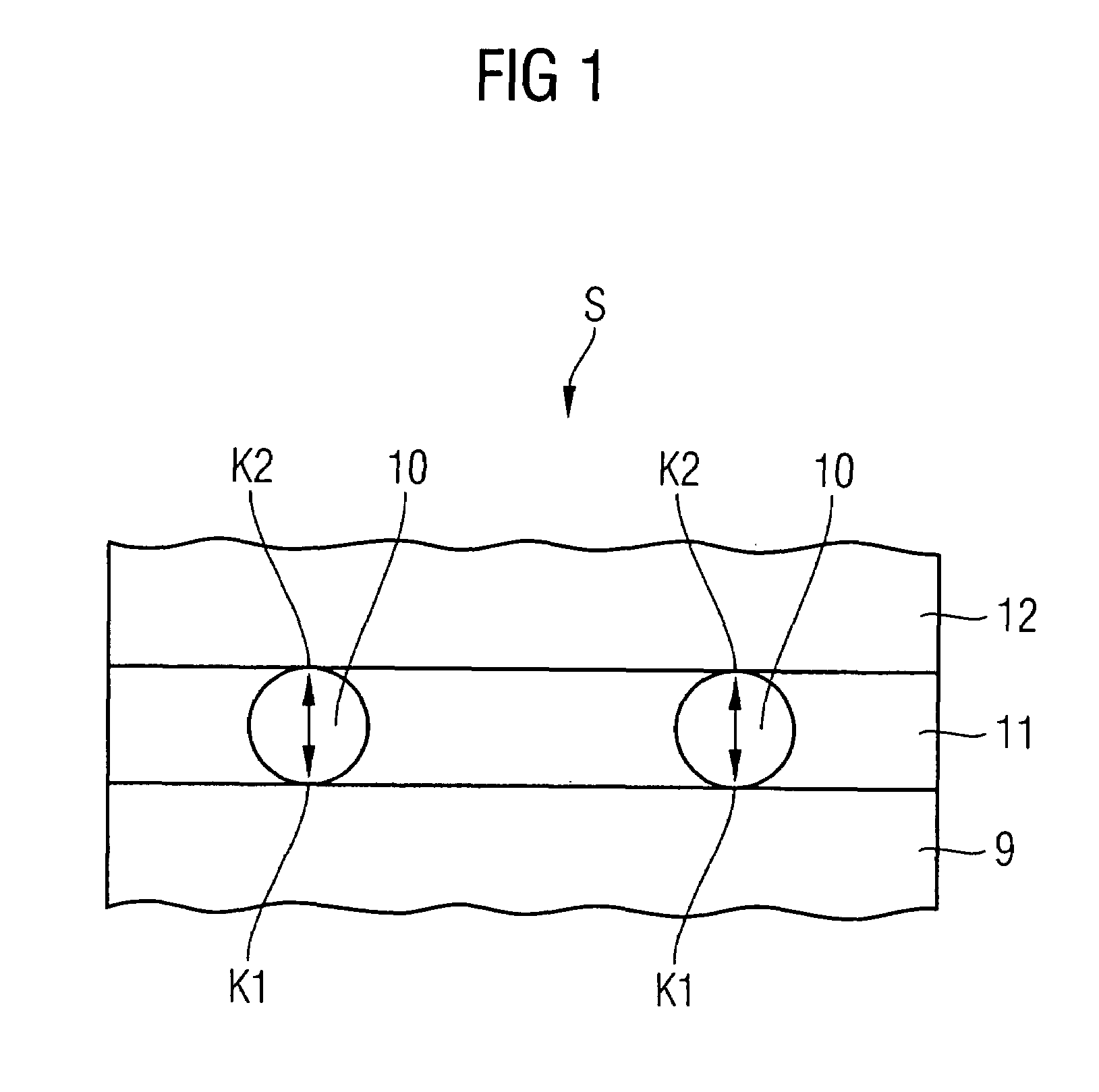
[0039]FIG. 1 illustrates a memory element S. Two nanoparticles 10 of, for example, NiO1−x are embedded in an isolating matrix 11 of a dielectric. The nanoparticles 10 contact a bottom contact 9 via contact locations K1 and a top contact 12 via contact locations K2.

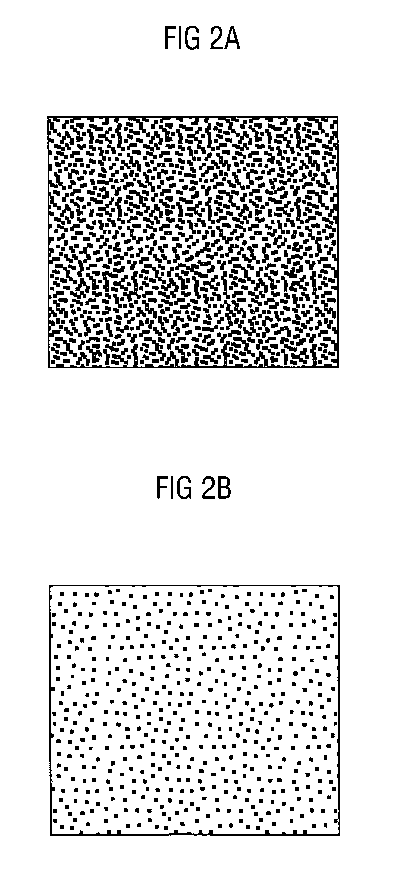
[0040]FIGS. 2a and 2b illustrate a nanoparticle structure with a particle size of 2.9 nm and 7.9 nm, respectively, manufactured in accordance with the embodiment.

[0041]FIG. 3 shows a NiO1−x nanoparticle 10 in an isolating matrix 11 without (left) and with (right) conductive filament. The nanoparticle is contacted by the bottom electrode 9 and the top electrode 12.

[0042]FIGS. 4 and 5 illustrate the configuration of a memory element array. FIG. 4 shows a top view of a memory element array. Word lines 9-1, 9-2 and 9-3 as well as bit lines 12-1, 12-2 and 12-3 are arranged on a substrate 1 made of e.g. silicon. An isolating matrix 11 in which nanoparticles are embedded is arranged between the word lines and the bit lines. The i...


PUM

PropertyMeasurementUnit
band gapaaaaaaaaaa
sizeaaaaaaaaaa
sizeaaaaaaaaaa

Abstract

Disclosed is a non-volatile memory cell including a first conductive electrode region, a second conductive electrode region and a memory region disposed therebetween. The memory region includes one or a plurality of metal oxide nanoparticles, which contact and electrically connect the first and the second electrode region via contact locations and which exhibit a bistable resistance properties when applying an external voltage.

Description

TECHNICAL FIELD[0001]The present invention relates to non-volatile, resistive memory cells based on the bistable resistance properties of metal oxide nanoparticles, a process for manufacturing such a non-volatile memory cell and an arrangement of a plurality of such memory cells to a memory cell arrangement.BACKGROUND ART[0002]Conventional storage technologies (floating gate memories such as flash and DRAM) are based on the storage of charges in inorganic, silicon-based materials. These technologies for storing electric charges will reach their scaling limits within the near future. Thus, there is increased research for alternative methods for storing information. Herein, the principle of resistive memories based on the bistable resistance change in metal oxide nanoparticles has proven to be promising.[0003]However, with conventional methods for manufacturing resistively switching metal oxide storage materials, active memory cells of few nanometers in dimension are unattainable. The...

Claims


Application Information

Patent Timeline
Patent Type & Authority Patents(United States)
IPC IPC(8): H01L29/02G11C11/00
CPCB82Y10/00B82Y30/00H01L27/2472H01L45/1608H01L45/1233H01L45/146H01L45/04H01L45/085H10B63/82H10N70/245H10N70/20H10N70/021H10N70/8833H10N70/826
Inventor UFERT, KLAUS
Owner POLARIS INNOVATIONS LTD
Why Eureka
Try Eureka