Delay locked loop circuit

a loop circuit and delay technology, applied in the field of delay lock loop circuits, can solve the problems of more power consumption, and achieve the effects of reducing the frequency, prolonging the delay time of the delay selection part, and increasing the frequency of external clock signals

Active Publication Date: 2007-11-20
SK HYNIX INC
View PDF5 Cites 22 Cited by
  • Summary
  • Abstract
  • Description
  • Claims
  • Application Information

AI Technical Summary

Benefits of technology

[0027]Accordingly, the present invention has been made to solve the above-mentioned problems occurring in the prior art, and an object of the present invention is to provide a delay locked loop circuit having a fast locking function and a relatively reduced delay line area.
[0032]According to the present invention, the higher the frequency of the external clock signal is as compared with the reference frequency range, the longer the delay time of the delay selection part determined by the second control signal group is, and the lower the frequency of the external clock signal is as compared with the reference frequency range, the shorter the delay time of the delay selection part determined by the second control signal group is.

Problems solved by technology

1. It is necessary to increase the number of unit delay circuits included in the delay line 102 in order to operate the delay locked loop circuit in a wide frequency band.
2. If the number of the unit delay circuits is increased, an area occupied by the delay line 102 is large.
3. The more the number of the unit delay circuits is, the more the power consumption is.

Method used


Image

  • Delay locked loop circuit
  • Delay locked loop circuit
  • Delay locked loop circuit

Examples


Embodiment Construction

[0039]Hereinafter, a preferred embodiment of the present invention will be described with reference to the accompanying drawings. In the following description and drawings, the same reference numerals are used to designate the same or similar components, and so repetition of the description on the same or similar components will be omitted.

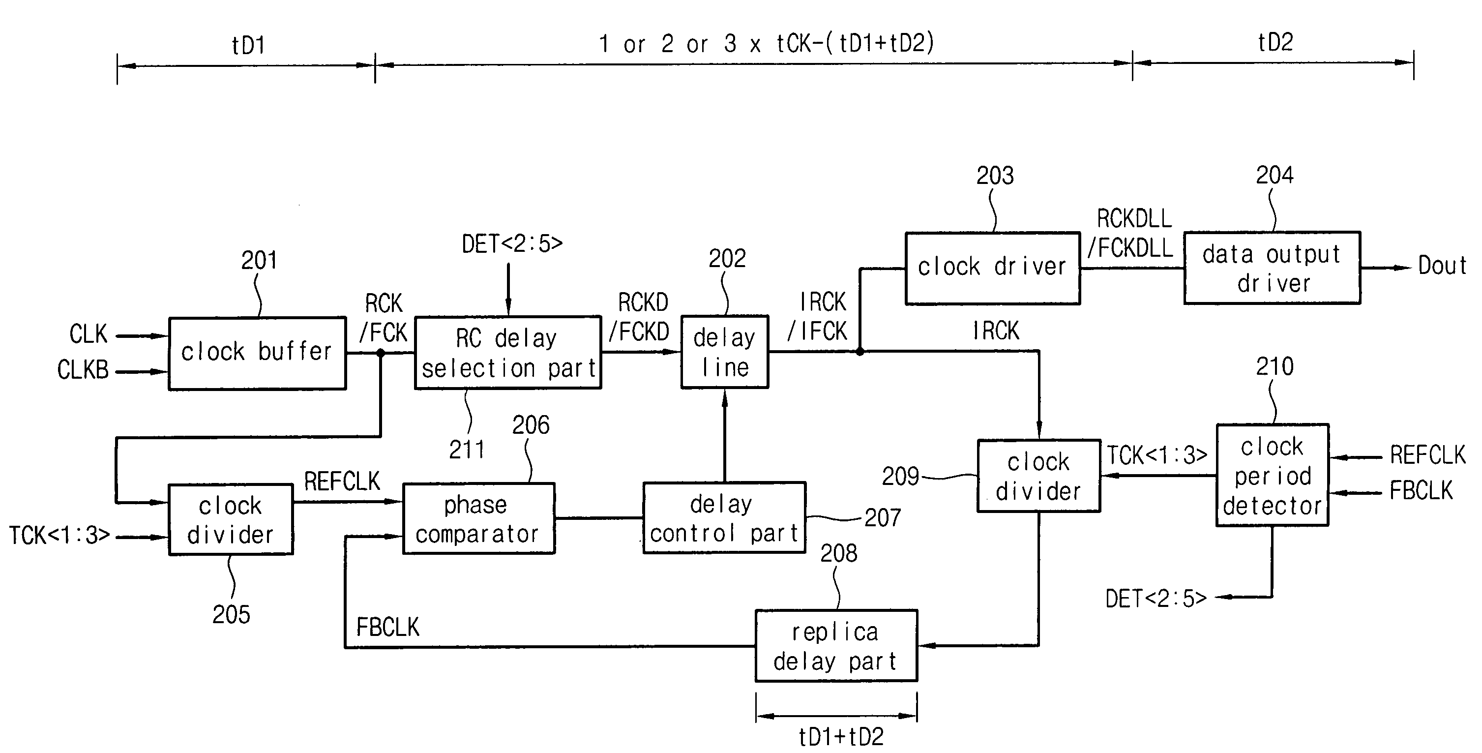
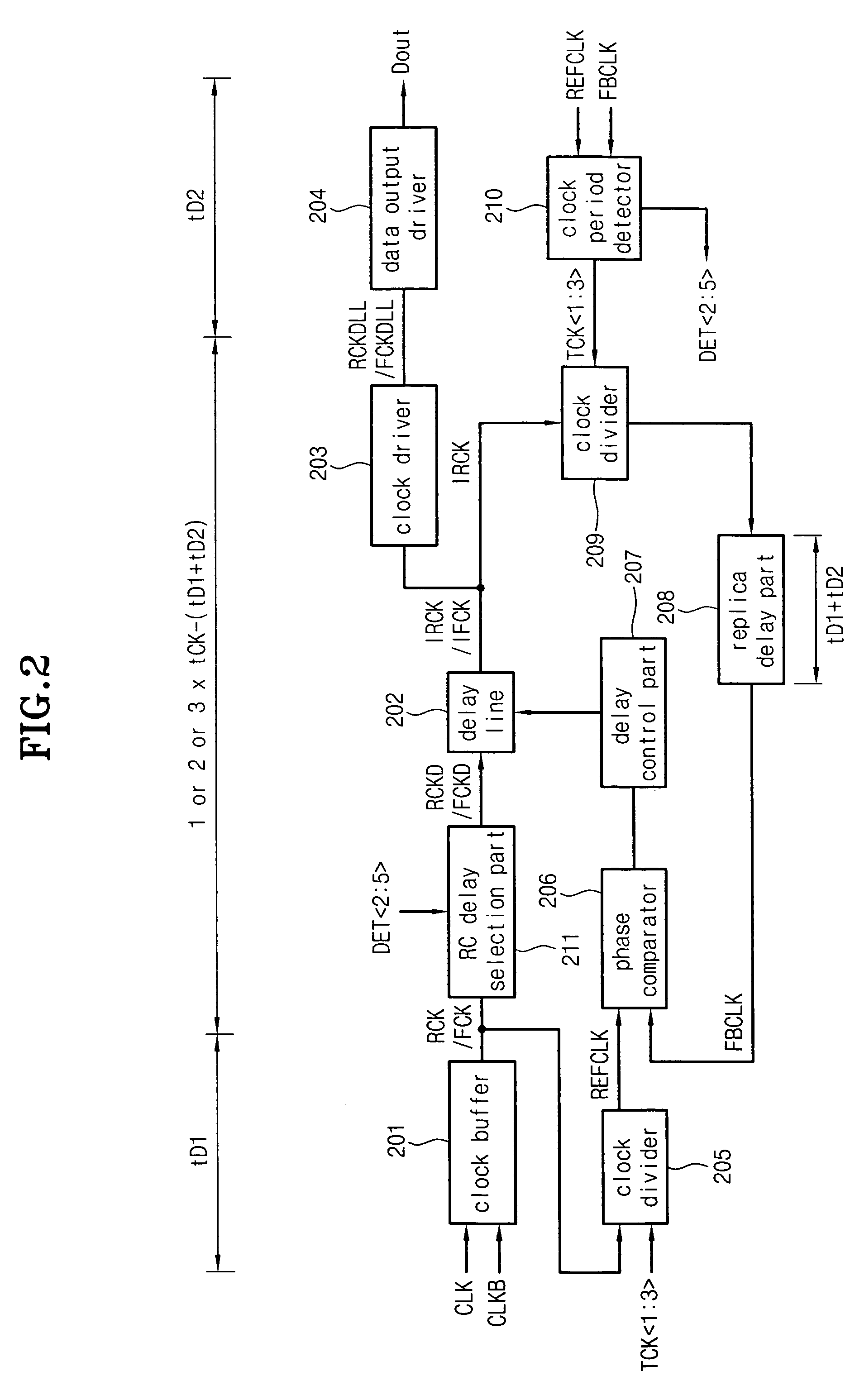
[0040]FIG. 2 illustrates an example of a delay locked loop circuit according to the present invention.

[0041]As shown in FIG. 2, the delay locked loop circuit according to the present invention includes a clock buffer 201 for receiving external clock signals CLK and CLKB, an RC delay selecting part 211 for receiving an output signal of the clock buffer 201 and delaying RC, a delay line 202 for receiving an output signal RCKD or FCKD of the RC delay selection part 211, a clock divider 205 for dividing an output signal of the clock buffer 201, a clock divider 209 for dividing an output signal (IRCK) from among output signals IRCK and IFCK of the dela...


PUM


Abstract

The DLL circuit detects a frequency of an external clock signal and adjusts a coarse delay during a DLL circuit operation, thereby quickly terminating a feedback operation of the DLL circuit and having a reduced circuit area of a delay line. Therefore, the DLL circuit can be used for next generation high-integration and high-frequency memory devices such as DDR2 SDRAMs.

Description

BACKGROUND OF THE INVENTION[0001]1. Field of the Invention[0002]The present invention relates to a delay locked loop circuit, and more particularly to a delay locked loop circuit having an improved processing speed and a reduced area for elements of the circuit, so that the delay locked loop circuit can operate in a wide range of a frequency through.[0003]2. Description of the Prior Art[0004]As generally known in the art, a semiconductor memory device has a phase difference between an externally inputted clock (external clock) and an internal clock due to several causes. That is, a phase of the external clock is delayed due to line loading and a clock input buffer receiving the external clock inputted into the semiconductor memory device. Also, a phase of the external clock is delayed due to line loading, an output buffer which receives internal cell data in order to output the internal cell data to the outside of the semiconductor memory device, and other logic circuits. As describ...

Claims


Application Information

Patent Timeline
Patent Type & Authority Patents(United States)
IPC IPC(8): H03L7/06G11C8/00G11C11/4076H03K5/13H03L7/081
CPCH03L7/0818A47G19/2222A47G21/181
Inventor KANG, YONG GUCHUN, JUN HYUN
Owner SK HYNIX INC
Why Eureka
Try Eureka