Page buffer and multi-state nonvolatile memory device including the same

a nonvolatile memory and buffer technology, applied in static storage, digital storage, instruments, etc., can solve the problems of numerous challenges and complex detection of multiple bits of multi-bit nonvolatile memory

Active Publication Date: 2007-11-20
SAMSUNG ELECTRONICS CO LTD
View PDF6 Cites 37 Cited by
  • Summary
  • Abstract
  • Description
  • Claims
  • Application Information

AI Technical Summary

Problems solved by technology

As should be apparent from the above, detection of the multiple bits of a multi-bit nonvolatile memory is quite complex when compared to the detection of a single-bit nonvolatile memory.
Numerous challenges are encountered when designing and developing the circuitry needed to both program and read the multiple bits from individual cell transistors.

Method used


Image

  • Page buffer and multi-state nonvolatile memory device including the same
  • Page buffer and multi-state nonvolatile memory device including the same
  • Page buffer and multi-state nonvolatile memory device including the same

Examples


Embodiment Construction

[0049]The present invention will now be described by way of preferred but non-limiting embodiments of the invention.

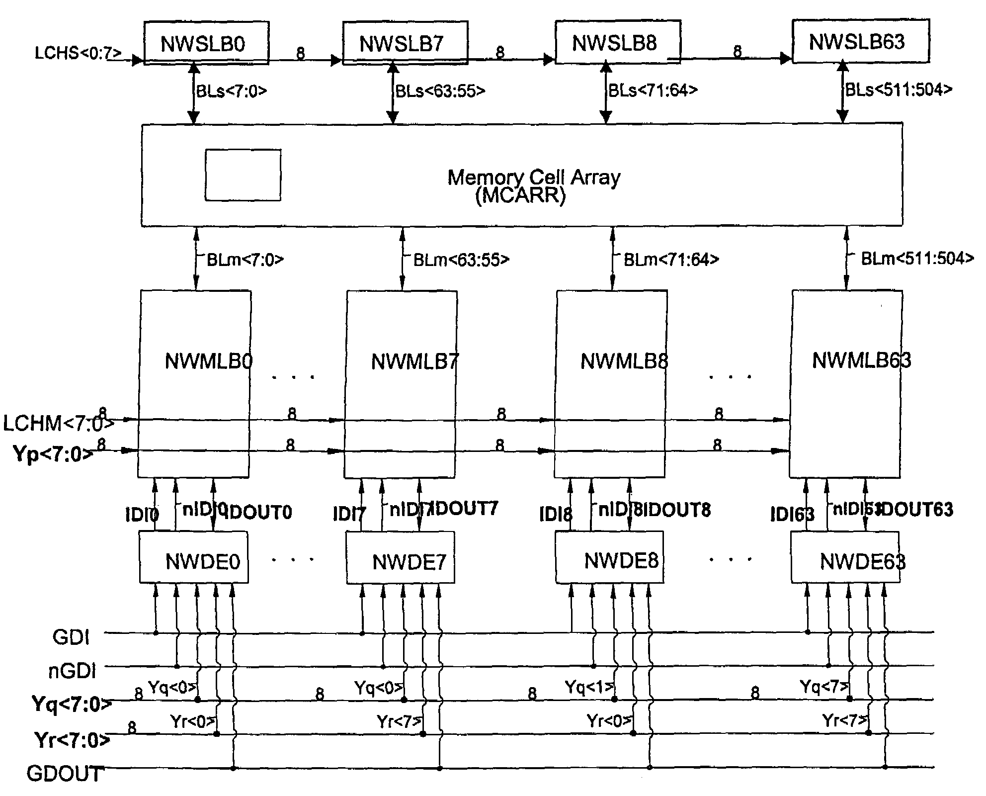
[0050]FIG. 8 is a schematic block diagram of a nonvolatile semiconductor memory device according to an embodiment of the present invention.

[0051]Referring to FIG. 8, the nonvolatile semiconductor memory device of this example includes a memory cell array MCARR, main latch blocks NWMLB63:0>, sub-latch blocks NWSLB63:0>, first and second global input lines GDI and nGDI, a global output line GDOUT, y address signal lines Yp7:0>, Yq7:0> and Yr7:0>, main read latch signal lines LCHM7:0>, sub-read latch signal lines LCHS7:0>, and page buffer decoders NWDE63:0>.

[0052]The memory cell array MCARR includes a matrix array of memory cells, word lines WL and bit lines BL. In the example of this embodiment, the memory cells are NAND flash memory cell transistors.

[0053]Internal input lines IDI63:0> and nIDI63:0>, and internal output lines IDOUT63:0>, are connected between the page bu...


PUM


Abstract

According to one aspect, a memory cell array includes a bit line connected to a plurality of nonvolatile memory cells, where the nonvolatile memory cells are selectively programmable in any one of at least first, second, third and fourth threshold voltage states, and where the first, second, third and fourth threshold voltage states correspond to four different data values defined by first and second bits. A page buffer circuit stores a logic value as main latch data and is responsive to a main latch signal to selectively flip the logic value of the main latch data according to a voltage level of the bit line. A sub-latch circuit stores a logic value as sub-latch data and is responsive to a sub-latch signal to selectively flip the logic value of the sub-latch data according to the voltage level of the bit line. The memory device is operable in a read mode which reads the threshold voltage state of the non-volatile memory cells and a programming mode which programs the threshold voltage state of the non-volatile memory cells, wherein the page buffer circuit is selectively responsive to the sub-latch data to inhibit flipping of the logic value of the main latch data in the programming mode.

Description

BACKGROUND OF THE INVENTION[0001]1. Field of the Invention[0002]The present invention generally relates to semiconductor memory devices, and more particularly, the present invention relates to nonvolatile semiconductor memory devices and to methods of operating nonvolatile memory devices.[0003]2. Description of the Related Art[0004]The demand for electrically programmable and electrically erasable nonvolatile memory devices has increased dramatically in recent years. Such devices are at least partially characterized by the ability to maintain stored data even in the absence of supplied power. The use of so-called flash memories has become especially popular, particularly, but not exclusively, in the context of portable devices such as digital cameras, cell phones, personal data assistants (PDAs), and laptop computers. Flash memories, such as NAND-type flash memories, are capable of storing large amounts of data in a relatively small area.[0005]As background discussion, the basic ope...

Claims


Application Information

Patent Timeline
Patent Type & Authority Patents(United States)
IPC IPC(8): G11C16/04
CPCG11C11/5628G11C11/5642G11C16/10G11C16/0483G11C2211/5642G11C16/24G11C16/26G11C16/34
Inventor LEE, SUNG-SOOLIM, YOUNG-HOCHO, HYUN-CHULCHAE, DONG-HYUK
Owner SAMSUNG ELECTRONICS CO LTD
Why Eureka
Try Eureka