
Method for producing a semiconductor component having a movable mass in particular, and semiconductor component produced according to this method

Inactive Publication Date: 2007-11-27
ROBERT BOSCH GMBH
View PDF12 Cites 14 Cited by
  • Summary
  • Abstract
  • Description
  • Claims
  • Application Information

AI Technical Summary

Benefits of technology

[0005]An example embodiment of the method according to the present invention may have the advantage over the related art that a micromechanical component having monocrystalline oscillator structures, e.g., an acceleration sensor or a rotational rate sensor, may be produced easily and inexpensively by surface micromechanics.

Problems solved by technology

Surface micromechanics for production of acceleration sensors or rotational rate sensors may be complex and therefore expensive.
Furthermore, they may have inferior long-term stability.
The methods of producing such sensors by surface micromechanics are not generally compatible with the typical methods of producing semiconductor circuit elements.

Method used


Image

  • Method for producing a semiconductor component having a movable mass in particular, and semiconductor component produced according to this method
  • Method for producing a semiconductor component having a movable mass in particular, and semiconductor component produced according to this method
  • Method for producing a semiconductor component having a movable mass in particular, and semiconductor component produced according to this method

Examples


Embodiment Construction

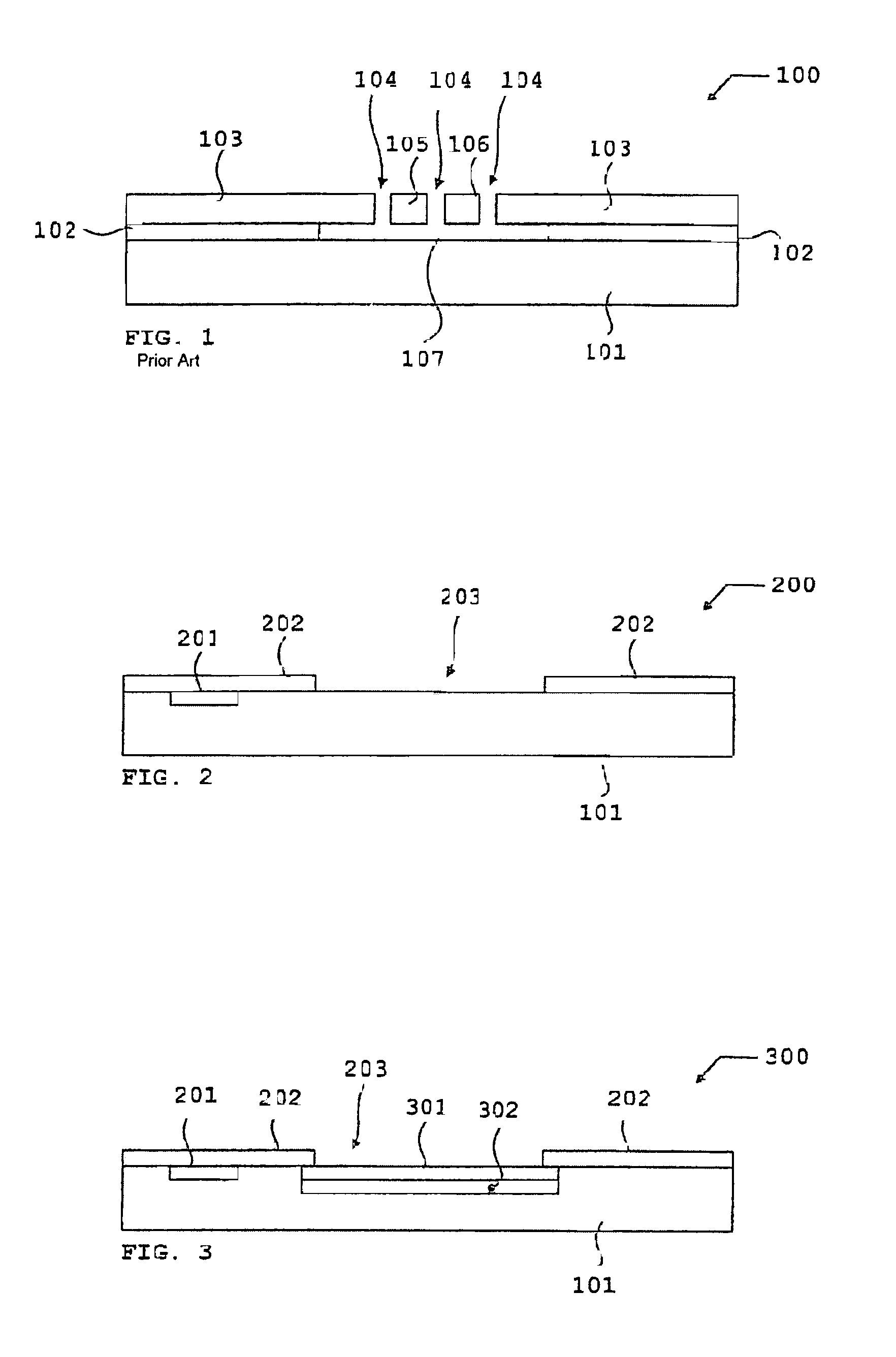
[0046]FIG. 1 shows precursor 100 of a known acceleration sensor. Precursor 100 has a silicon substrate 101 of monocrystalline silicon, a sacrificial silicon oxide layer 102 deposited on silicon substrate 101 and a polysilicon layer 103 of polycrystalline silicon deposited on sacrificial silicon oxide layer 102. An etching mask (not shown) is applied to precursor 100 in a known way, so that etching openings 104 are not covered by the etching mask. The top side of precursor 100 shown in FIG. 1 is subsequently etched in a known way, thus creating, i.e., forming, mobile masses 105 and 106 in polysilicon layer 103 and a cavern, i.e., a cavity 107 in sacrificial silicon oxide layer 102, as shown in FIG. 1.

[0047]One disadvantage of this method of producing precursor 100 of a conventional acceleration sensor as shown in FIG. 1 is that the mobile masses have fluctuations in their mechanical properties in mass production due to the polysilicon structure. Furthermore, there are great fluctuati...


PUM

PropertyMeasurementUnit
Fractionaaaaaaaaaa
Fractionaaaaaaaaaa
Porosityaaaaaaaaaa

Abstract

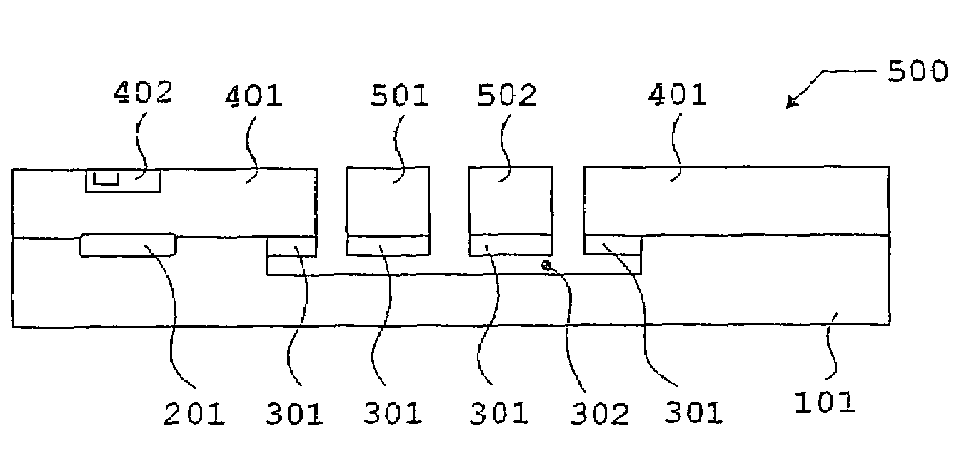
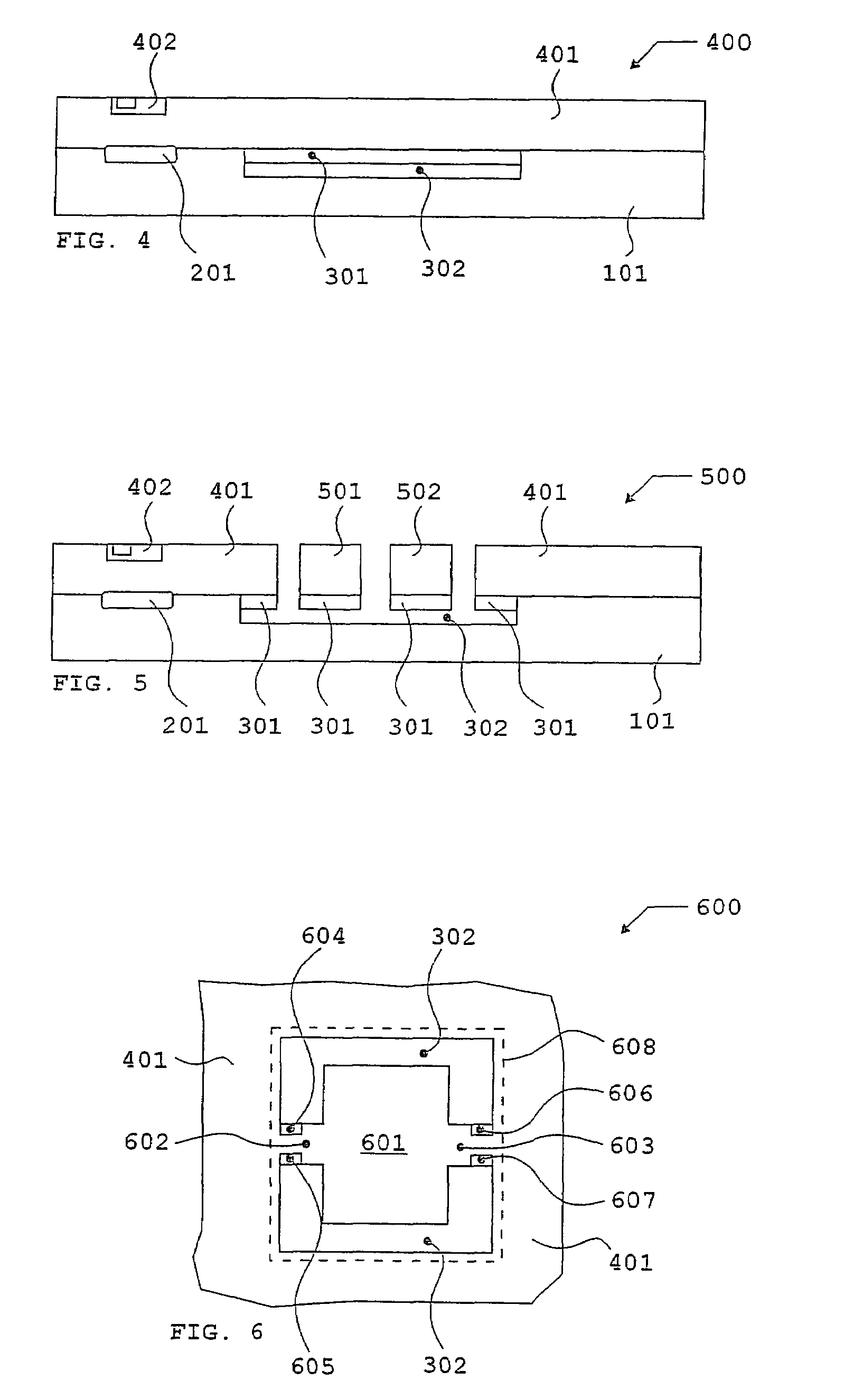
A method of producing a semiconductor component, e.g., a multilayer semiconductor component, and a semiconductor component produced by this method, where the semiconductor component has, e.g., a mobile mass, i.e., an oscillator structure.A method easily and inexpensively produce a micromechanical component having monocrystalline oscillator structures, such as an acceleration sensor or a rotational rate sensor for example, by surface micromechanics, a first porous layer is formed in the semiconductor component in a first step and a cavity, i.e., a cavern, is formed beneath or out of the first porous layer in the semiconductor component in a second step.

Description

BACKGROUND INFORMATION[0001]The present invention is directed to a method for producing a semiconductor component, e.g., a multilayer semiconductor component, and to a semiconductor component produced by this method, the semiconductor component having a mobile mass, i.e., an oscillator structure.[0002]Some semiconductor components such as micromechanical acceleration sensors or rotational rate sensors in particular have a mobile mass, i.e., an oscillator structure. Such sensors are usually produced from polycrystalline silicon by surface micromechanics, the oscillator structure being created by etching away a sacrificial silicon oxide layer by gas phase etching so the oscillator structure is freely mobile.[0003]Surface micromechanics for production of acceleration sensors or rotational rate sensors may be complex and therefore expensive. In comparison with an oscillator structure of monocrystalline silicon, it may be possible to produce oscillator structures of polycrystalline silic...

Claims


Application Information

Patent Timeline
IPC IPC(8): H01L21/76H01L21/00H01L21/20G01P9/04B81B3/00B81C1/00C23F1/24G01C19/56G01P15/12H01L21/306H01L29/84
CPCB81C1/00492B81B2201/0235B81B2203/0315Y10S438/96B81C2201/0115H01L29/84
Inventor BENZEL, HUBERTWEBER, HERIBERTSCHAEFER, FRANK
Owner ROBERT BOSCH GMBH
Learn More