Image display device and driver circuit therefor

a driver circuit and image display technology, applied in the direction of instruments, static indicating devices, etc., can solve the problems of large amount of data, serious obstacles, and large occupied area of the digital system driver circuit as described above, so as to reduce the delay of a digital picture signal and the waveform distortion thereof, reduce the number of storage circuits, and reduce the occupied area of the signal line driver circui

Inactive Publication Date: 2007-11-27
SEMICON ENERGY LAB CO LTD
View PDF40 Cites 23 Cited by
  • Summary
  • Abstract
  • Description
  • Claims
  • Application Information

AI Technical Summary

Benefits of technology

[0020]Then, for the purpose of solving the foregoing problems, the present invention has an object to provide a technique for reducing an occupied area of a signal line driver circuit and further to reduce the delay of a digital picture signal and the waveform distortion thereof.
[0021]Storage circuits and D / A converter circuits in a signal line driver circuit are jointly owned by n (n is a natural number not less than 2) signal lines, respectively. One horizontal scan period is divided into n periods, and the storage circuits and the D / A converter circuits perform a processing to the different signal lines in the divided respective periods, so that all the signal lines can be driven equally to the related art. In this way, it becomes possible to decrease the number of the storage circuits and that of the D / A converter circuits in the signal line driver circuit to 1 / n of that of the related art. Incidentally, in the present specification, to perform a suitable processing to the signal line or the scan line for displaying an image is expressed by “to drive the signal line” or “to drive the scan line”.
[0022]The digital picture signal is directly inputted to a shift register and is sequentially shifted in the shift register, and when it reaches a desired position, input of a clock signal is stopped to cease shifting the signal, and the signal is held at that position. A latch signal is inputted before the input of a next digital picture signal and a clock signal starts, so that the signal held in the shift register is transferred to the storage circuit, and whereby an operation equal to that up to the second storage circuit of the related art can be performed. Like this, by directly inputting the digital picture signal to the shift register, the signal transmission line for supplying the digital picture signal is shortened and the number of gates to be connected becomes several from several thousand, so that the gate capacitance becomes dramatically small, and it becomes possible to decrease the resistance and load capacitance of the signal transmission line.

Problems solved by technology

As compared with an analog system, the digital system driver circuit as described above has a defect that its occupied area is very large.
Although the digital system has a merit that a signal can be expressed by two values of “Hi” and “Lo”, the amount of data becomes large instead, and it becomes a serious obstacle from the viewpoint of miniaturization in constructing the image display device.
The increase in area of the image display device has problems that the increase in its manufacturing costs is caused and the profit of a manufacturing company is made worse.
As a result, a load to the signal transmission line, such as load capacitance or resistance, becomes large, and the delay of the digital picture signal and the waveform distortion become large.
This tendency becomes remarkable when the number of pixels increases, and there occurs a problem that a display based on accurate digital picture signals becomes difficult.

Method used


Image

  • Image display device and driver circuit therefor
  • Image display device and driver circuit therefor
  • Image display device and driver circuit therefor

Examples


embodiment 1

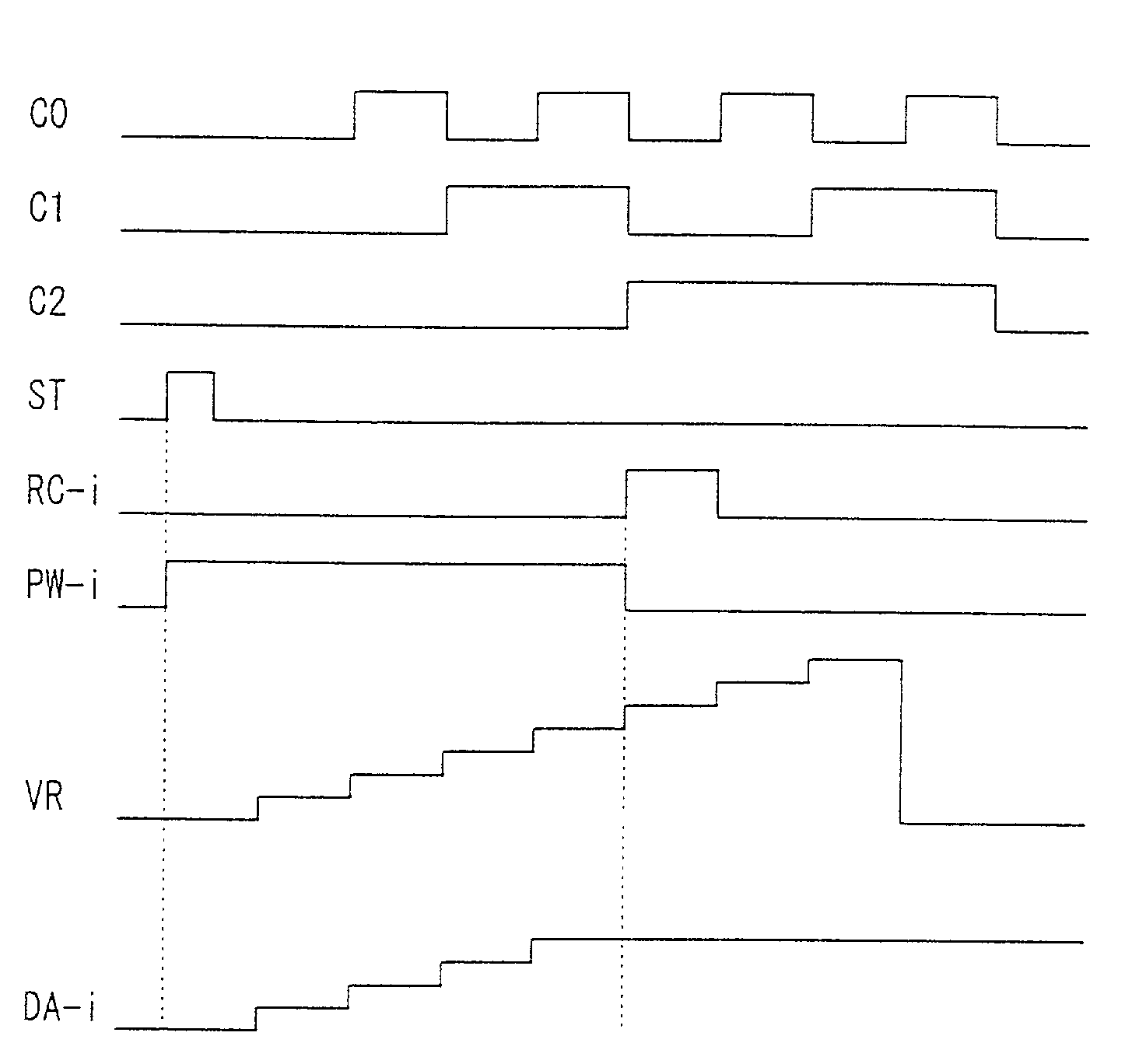
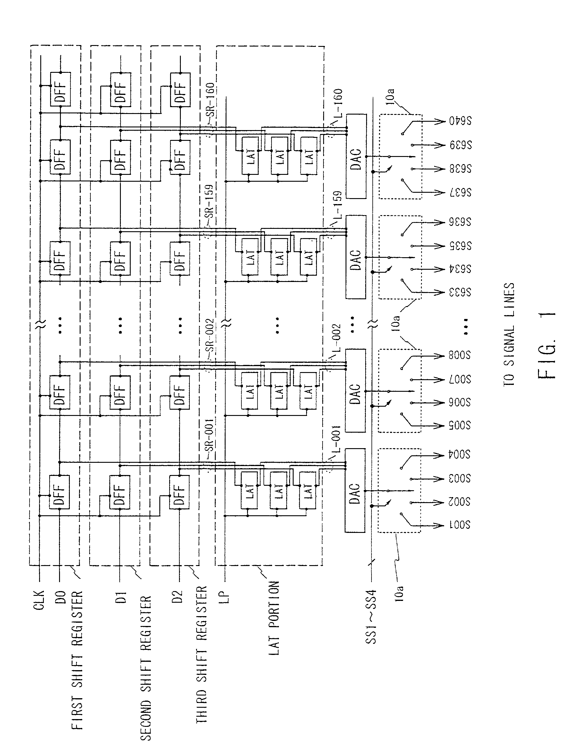
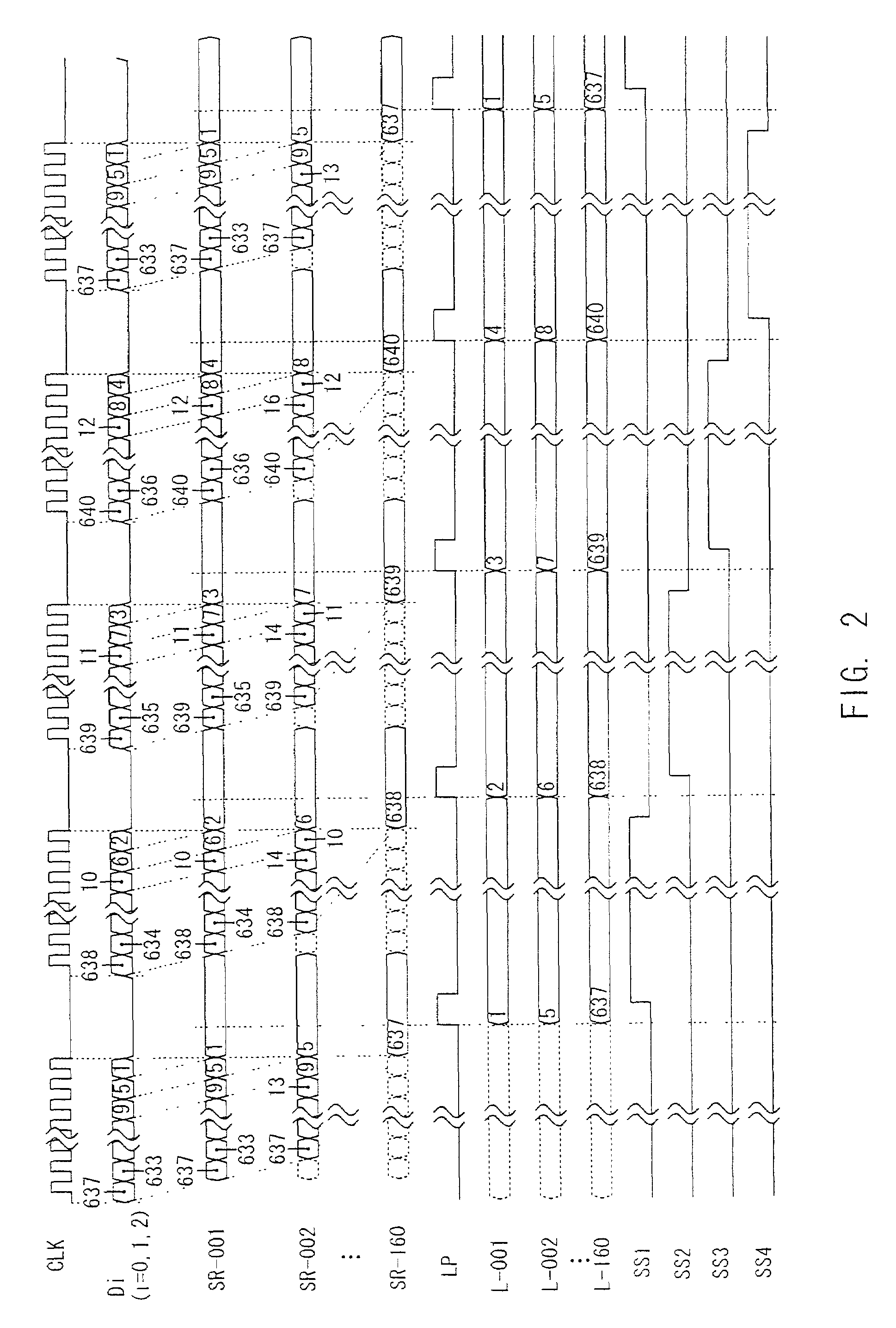
[0071]In this embodiment, an image display device of the XGA standard in which the number of pixels in the horizontal direction is 1024 and the number of pixels in the vertical direction is 768, will be described. In this embodiment although the description will be made on the assumption that a digital picture signal has 3 bits, the present invention is not limited to 3 bits, but is also effective for 6 bits, 8 bits, or a bit number other than those. Besides, a case where one D / A converter circuit drives four signal lines will be exemplified.

[0072]Hereinafter, the structure of this embodiment will be described, and next, the operation of this embodiment will be described.

[0073]FIG. 3 shows a signal line driver circuit according to this embodiment. Since the structure of a scan line driver circuit and the structure of a pixel array portion are the same as the related art, their explanation is omitted. The signal line driver circuit of this embodiment includes three shift registers (f...

embodiment 2

[0092]In this embodiment, an example of a case where a ramp system D / A converter circuit is adopted for a D / A converter circuit, will be described. FIG. 6 is a schematic view of a signal line driver circuit in the case where the ramp system D / A converter circuit is used. Incidentally, also in this embodiment, although the description will be made on a case corresponding to the image display device of the XGA standard and a 3-bit digital picture signal, the present invention is not limited to the 3 bits, but is also effective for a case corresponding to another bit number or the image display device of a standard other than the XGA.

[0093]The structure and operation of the embodiment will hereinafter be described.

[0094]In this embodiment, the structure from shift registers to storage circuits (LAT) is the same as the embodiment 1. At the downstream of the storage circuits. there are provided bit comparison pulse width converter circuits (BPC), analog switches 20. and signal line selec...

embodiment 3

[0101]In this embodiment, a description will be made on an example of a color image display device which is a single plate of the VGA standard in which the number of pixels in the horizontal direction is 640×3 (three colors of RGB) and the number of pixels in the vertical direction is 480, and can produce a color display. R, G and B indicate red, green and blue of the three primary colors of light, respectively. Also in this embodiment, although the description is made on the assumption that a digital picture signal has three bits, the present invention is not limited to 3 bits, but is also effective for 6 bits, 8 bits or a bit number other than those. Besides, a case where one D / A converter circuit drives three signal lines is cited as an example.

[0102]The structure and operation of the embodiment will hereinafter be described.

[0103]FIG. 10 shows a signal line driver circuit according to this embodiment. Since the structure of a scan line driver circuit and the structure of a pixel...


PUM


Abstract

There is provided an image display device operating in response to the input of digital picture signals, in which the occupied area of a signal line driver circuit thereof is reduced, and the parasitic capacitance and resistance of input transmission lines of the digital picture signals are reduced. The device includes both a unit for directly inputting the digital picture signals to shift registers and for performing series parallel conversion, and a unit for causing n (n is a natural number not less than 2) signal lines to jointly own storage circuits and D/A converter circuits in the signal line driver circuit. One horizontal scan period is divided into n periods, and the storage circuits and the D/A converter circuits perform a processing to signal lines different in each of the divided periods.

Description

BACKGROUND OF THE INVENTION[0001]1. Field of the Invention[0002]The present invention relates to an image display device to which a digital picture signal is inputted and a driver circuit therefore. More particularly, the present invention is directed to a driver circuit for an image display device in which an occupied area of the driver circuit is reduced, and further. the delay of a digital picture signal to be inputted and the waveform distortion thereof are reduced.[0003]2. Description of the Related Art[0004]In recent years, an image display device in which semiconductor thin films are formed on a glass substrate, in particular an active matrix image display device using thin film transistors (hereinafter referred to as TFTs) has come into wide use. The active matrix image display device (hereinafter referred to as image display device) using the TFTs includes hundreds of thousand to several million TFTs arranged in a matrix form, which control electric charges of respective pi...

Claims


Application Information

Patent Timeline
Patent Type & Authority Patents(United States)
IPC IPC(8): G09G3/36G09G3/30
CPCG09G3/30G09G3/3648G09G2310/0297G09G2310/0259G09G2310/027G09G2300/0809
Inventor KOYAMA, JUNAZAMI, MUNEHIRO
Owner SEMICON ENERGY LAB CO LTD
Why Eureka
Try Eureka