Threshold voltage control layer in a semiconductor device

a technology of threshold voltage control and semiconductor devices, which is applied in the direction of semiconductor devices, electrical devices, transistors, etc., can solve the problems of difficult to achieve complete depletion and difficult to implant impurities into shallow portions below the end portion, and achieve the effect of improving current gain

Active Publication Date: 2007-12-04
GK BRIDGE 1
View PDF16 Cites 119 Cited by
  • Summary
  • Abstract
  • Description
  • Claims
  • Application Information

AI Technical Summary

Benefits of technology

[0011]In the semiconductor device according to the present invention, instead of the pocket implantation region provided under the extension region, the threshold voltage control layer is formed to maintain an impurity concentration which provides a desired threshold voltage at the surface of a channel under a gate insulating film, while having a concentration peak at a slightly deeper position. As a result, the enlargement of the extension region can be suppressed and even the portion of the channel region which is located below the drain-side end portion of the gate electrode is completed depleted. This allows the suppression of variations in channel length and increases the absolute value of an early voltage so that a high current gain is obtainable.

Problems solved by technology

However, since an impurity is normally implanted into the pocket implantation region by using the gate electrode as a mask, it is difficult to implant the impurity into a shallow portion below the end portion of the gate electrode such that the conductivity type of the LDD region is cancelled out.
Accordingly, the problem is encountered that complete depletion is hard to achieve.

Method used


Image

  • Threshold voltage control layer in a semiconductor device
  • Threshold voltage control layer in a semiconductor device
  • Threshold voltage control layer in a semiconductor device

Examples


Embodiment Construction

[0021]Referring to the drawings, an embodiment of the present invention will be described.

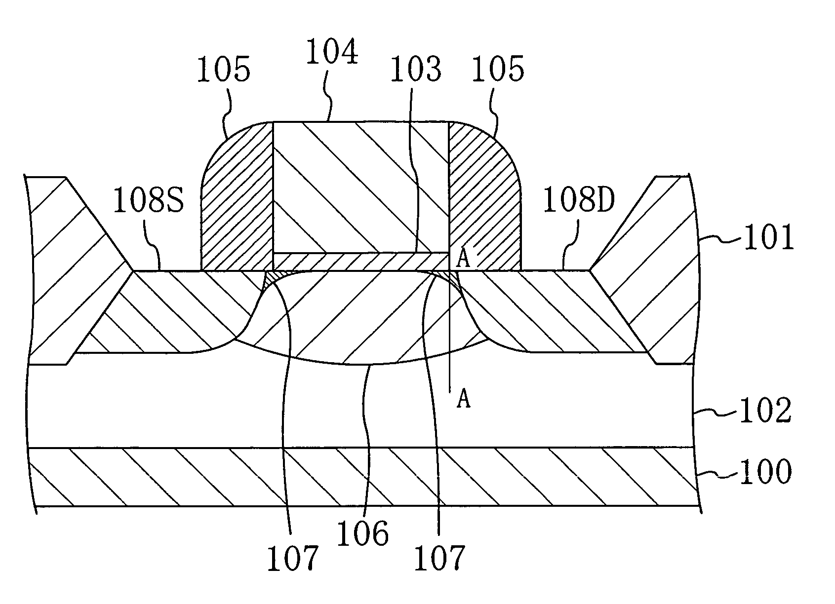
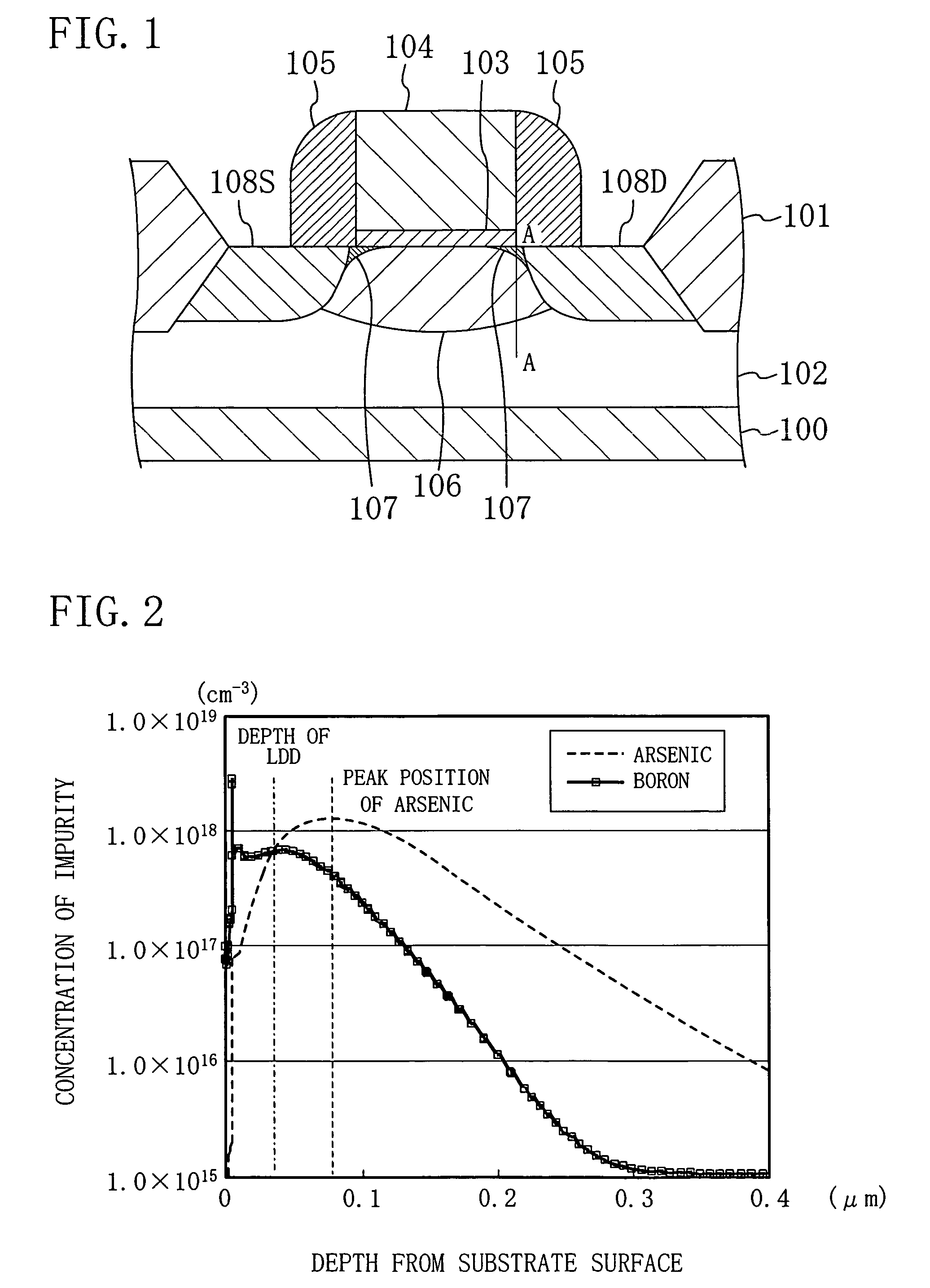
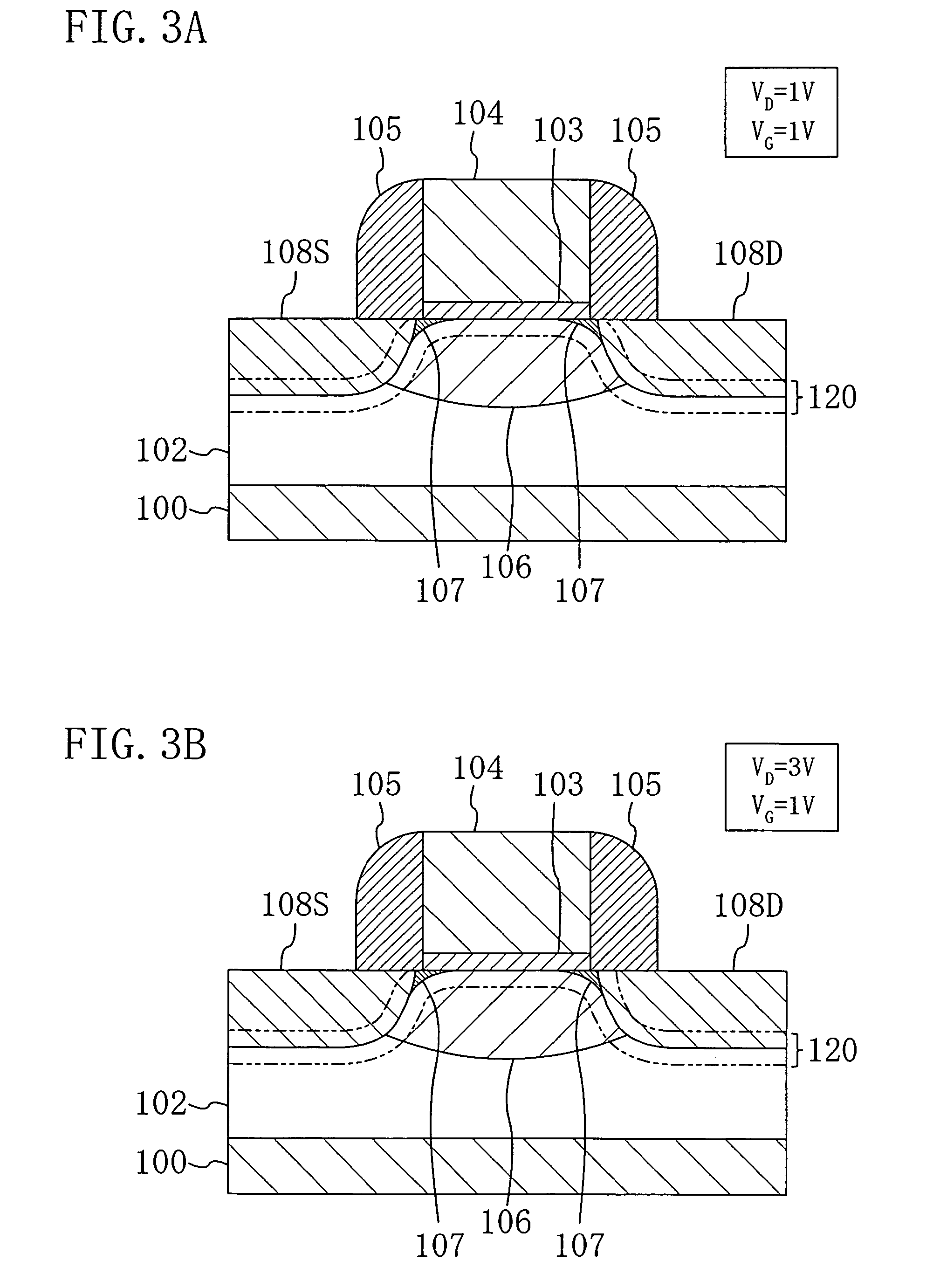
[0022]FIG. 1 schematically shows a cross-sectional structure of a MIS transistor as a semiconductor device according to the embodiment. As shown in FIG. 1, multiple isolation films 101 composed of silicon dioxide and an N-type well region 102 having a junction surface deeper than the respective bottom surfaces of the isolation films 101 are formed in an upper portion of a semiconductor substrate 100 made of, e.g., P-type silicon (Si).

[0023]On each of device formation regions of the principal surface of the semiconductor substrate 100 which are defined by the isolation films 101, there are formed a gate insulating film 103 made of silicon dioxide and having a thickness of, e.g., 6.5 nm and a gate electrode 104 made of polysilicon and having a thickness of, e.g., 280 nm and a gate length of, e.g., 370 nm. On the respective both side surfaces of the gate insulating film 103 and the gate electrode ...


PUM


Abstract

A semiconductor device has a well region having a first conductivity type and formed in an upper portion of a semiconductor substrate, a gate insulating film and a gate electrode formed successively on the well region of the semiconductor substrate, a threshold voltage control layer for controlling a threshold voltage formed in the portion of the well region which is located below the gate electrode and in which an impurity of the first conductivity type has a concentration peak at a position shallower than in the well region, an extension region having a second conductivity type and formed in the well region to be located between each of the respective portions of the well region which are located below the both end portions in the gate-length direction of the gate electrode and the threshold voltage control layer, and source and drain regions each having the second conductivity type and formed outside the extension layer in connected relation thereto. The junction surface between the threshold voltage control layer and the extension region has an upwardly protruding configuration.

Description

CROSS-REFERENCE TO RELATED APPLICATIONS[0001]The teachings of Japanese Patent Application JP 2005-256031, filed Sep. 5, 2005, are entirely incorporated herein by reference, inclusive of the claims, specification, and drawings.BACKGROUND OF THE INVENTION[0002]The present invention relates to a semiconductor device and a method for fabricating the same and, more particularly, to a MIS (metal insulator semiconductor) transistor having an extension structure and further having an LDD (lightly doped drain) structure in the source and drain regions thereof.[0003]In recent years, MIS-type analog-digital mixed LSIs (large scale integrated circuits) have been used to control electronic equipment. To provide a MIS-type analog-digital mixed LSI featuring higher-speed operation and higher integration, a CMIS (complementary MIS) analog circuit technology has been becoming important.[0004]In a CMIS analog circuit, the current gain gradually attenuates as the operational frequency is increased dur...

Claims


Application Information

Patent Timeline
Patent Type & Authority Patents(United States)
IPC IPC(8): H01L29/94
CPCH01L21/2253H01L21/26586H01L29/6659H01L29/7833H01L29/1079Y10S257/927
Inventor MISAKI, MAKOTO
Owner GK BRIDGE 1
Why Eureka
Try Eureka