Liquid-crystal display driving circuit and method

a liquid crystal display and driving circuit technology, applied in the direction of electric digital data processing, instruments, computing, etc., can solve the problems of large source-line driving circuits, increased current consumption, and increased time needed to charge the parasitic capacitance of source lines, so as to reduce electrical noise, reduce current consumption, and reduce the effect of driving capability

Inactive Publication Date: 2007-12-04
LAPIS SEMICON CO LTD
View PDF18 Cites 12 Cited by
  • Summary
  • Abstract
  • Description
  • Claims
  • Application Information

AI Technical Summary

Benefits of technology

[0006]It is accordingly an object of the present invention to reduce the current consumed in charging the parasitic capacitances of signal lines in a liquid-crystal display.
[0007]Another object of the invention is to reduce the time needed for charging the parasitic capacitances of signal lines in a liquid-crystal display.
[0008]Yet another object is to reduce electrical noise in a liquid-crystal display.
[0009]Still another object is to reduce the size and cost of the driving circuits of a liquid-crystal display.
[0016]The first and second aspects of the invention recycle charge from one signal line to another through the short circuits, thereby reducing current consumption, reducing electrical noise, and enabling the signal lines to be driven more rapidly, or to be driven by drivers with less driving capability, hence with smaller size and lower cost.
[0017]The third aspect of the invention provides similar effects by reducing the frequency with which the second signal lines are driven from one side of the center potential to the opposite side.

Problems solved by technology

A resulting problem is that the time needed to charge the parasitic capacitances of the source lines is increased, current consumption is similarly increased, and large source-line driving circuits are needed.
The large charging and discharging currents furthermore generate electrical noise.
Although the gate lines are not driven in an AC manner, they also have parasitic capacitances that must be charged and discharged.
The charging and discharging of the gate lines similarly takes time, consumes current, generates noise, and requires large driving circuits.

Method used


Image

  • Liquid-crystal display driving circuit and method
  • Liquid-crystal display driving circuit and method
  • Liquid-crystal display driving circuit and method

Examples


first embodiment

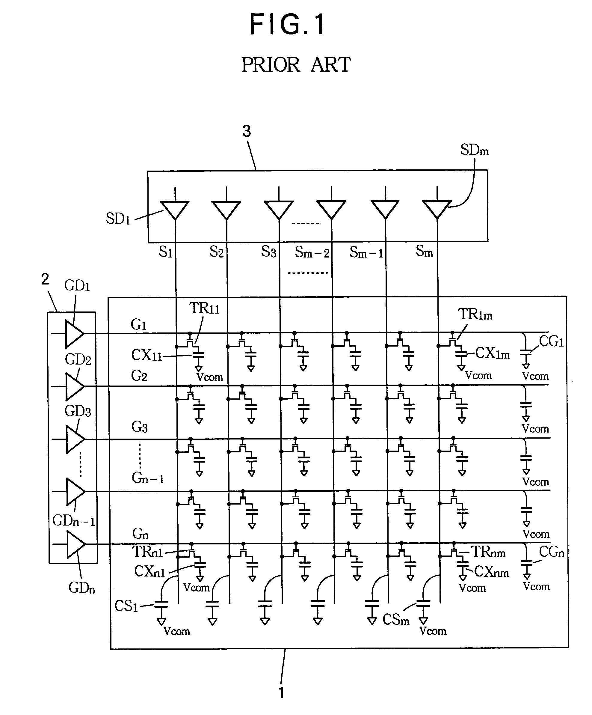
[0047]FIG. 4 shows the invention. The LCD panel 1 and gate-line driving circuit 2 are similar to the conventional elements shown in FIG. 1.

[0048]The source-line driving circuit 10 in the first embodiment has a switching circuit 11 comprising switches SWA1 to SWAm and SWB1 to SWBm. Switch SWAj couples source line Sj to source driver SDj (j=1, . . . , m), while switch SWBj couples source line Sj to a common electrode (not visible) held at the potential Vcom of the common electrode of the liquid-crystal capacitors. Switches SWAj and SWBj comprise, for example, field-effect transistors. This type of switching circuit 11 can easily be added to existing source-line driving circuit designs.

[0049]The switches SWAj and SWBj are controlled in synchronization with the gate drivers GD1 to GDn. Normally, switches SWAj are all closed, and switches SWBj are all open. At times of transition of the gate lines G1 to Gn between the high and low levels, however, for a brief interval switches SWAj are o...

second embodiment

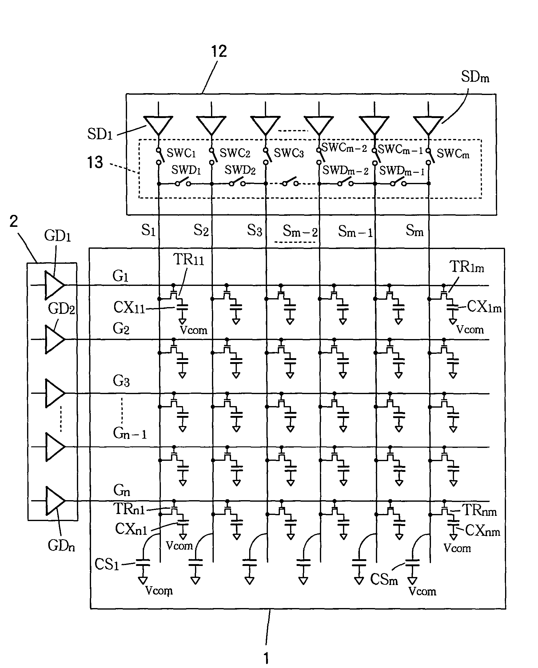
[0056]FIG. 5 shows the invention. The LCD panel 1 and gate-line driving circuit 2 are similar to the conventional elements in FIG. 1.

[0057]The source-line driving circuit 12 in the second embodiment has a switching circuit 13 comprising switches SWC1 to SWCm and SWD1 to SWDm−1. Switch SWCj couples source line Sj to source driver SDj (j=1, . . . , m), while switch SWDj couples source line Sj to source line Sj+1 (j=1, . . . , m−1). Switches SWCj and SWDj comprise, for example, field-effect transistors, and can easily be added to existing source-line driving circuit designs.

[0058]The control of switches SWCj and SWDj is analogous to the control of switches SWAj and SWBj in the first embodiment. Normally, switches SWCj are all closed, and switches SWDj are all open. At each transition of any of the gate lines G1 to Gn between the high and low levels, for a brief interval switches SWCj are opened, and switches SWDj are closed, thereby disconnecting the source lines from the source driver...

third embodiment

[0060]FIG. 6 shows the invention. The LCD panel 1 and gate-line driving circuit 2 are similar to the conventional elements in FIG. 1.

[0061]The source-line driving circuit 14 in the third embodiment has a switching circuit 15 comprising switches SWC1, SWC2, . . . , SWCm and SWD1, SWD3, . . . , SWDm−1. Switching circuit 15 is obtained from the switching circuit 13 of the second embodiment by removing the even-numbered switches SWD2, SWD4, . . . , SWDm−2 that short-circuit adjacent source lines.

[0062]The third embodiment operates in the same way as the second embodiment, but when switches SWChd j (j=1, 2, . . . , m) are opened and switches SWDj (j=1, 3, . . . , m−1) are closed, each source line is short-circuited to just one adjacent source line. Since adjacent source lines are driven to potentials on opposite sides of a center potential approximately equal to Vcom, each short-circuited pair of source lines is brought to a potential in the general vicinity of Vcom.

[0063]The third embod...


PUM

PropertyMeasurementUnit
capacitanceaaaaaaaaaa
speedaaaaaaaaaa

Abstract

A driving circuit for an active-matrix liquid-crystal display short-circuits at least two of the signal lines in the matrix at times of transitions of signal-line potentials in the matrix. Charge stored in the parasitic capacitances of the signal lines is thereby recycled from one signal line to another, reducing the current consumption of the driving circuit. When alternating-current driving is employed, current consumption can also be reduced by reducing the frequency with which signal lines are driven from one side of a center potential to the other side.

Description

[0001]This application is a continuation of application Ser. No. 09 / 718,620, which was filed on Nov. 24, 2000 now U.S. Pat. No. 6,642,916.BACKGROUND OF THE INVENTION[0002]The present invention relates to a circuit and method for driving a liquid-crystal display, such as an active-matrix display employing thin-film transistors.[0003]Active-matrix liquid-crystal displays or LCDs are widely employed in, for example, portable computers, where they provide the advantages of high-speed response and reduced crosstalk. In a typical active-matrix LCD, for each of the three primary colors, each picture element or pixel has a thin-film transistor (TFT) that is switched on and off by a signal received from a gate line, and a liquid-crystal capacitor that charges or discharges through a source line when the TFT is switched on. The source and gate lines form a matrix in which the gate lines are activated one at a time, and the source lines carry signals representing the displayed intensities of t...

Claims


Application Information

Patent Timeline
Patent Type & Authority Patents(United States)
IPC IPC(8): G09G3/36G02F1/133
CPCG09G3/3688G09G2330/021G09G2320/02G09G2310/0248
Inventor KODAMA, HIDETAKAKOKUDA, KENJIFURUYA, HIROSHI
Owner LAPIS SEMICON CO LTD
Why Eureka
Try Eureka