Lag control

a technology of lag control and semiconductor devices, which is applied in the manufacturing of basic electric elements, semiconductor/solid-state devices, electric devices, etc., can solve the problems of slow operation of semiconductor devices, and achieve the effect of slow and faster etching of small features

Active Publication Date: 2007-12-11
LAM RES CORP
View PDF6 Cites 28 Cited by
  • Summary
  • Abstract
  • Description
  • Claims
  • Application Information

AI Technical Summary

Benefits of technology

[0008]To achieve the foregoing and in accordance with the purpose of the present invention a method for etching features in a silicon oxide based dielectric layer over a substrate, comprising performing an etch cycle is provided. A lag etch partially etching features in the silicon oxide based dielectric layer is performed, which comprises providing a lag etchant gas, forming a plasma from the lag etchant gas, and etching the etch layer with the lag etchant gas, so that smaller features are etched slower than wider features. A reverse lag etch further etching the features in the silicon oxide based dielectric layer is performed comprising providing a reverse lag etchant gas, which is different from the lag etchant gas and is more polymerizing than the lag etchant gas, forming a plasma from the reverse lag etchant gas, and etching the silicon oxide based dielectric layer with the plasma formed from the reverse lag etchant gas, so that smaller features are etched faster than wider features.

Problems solved by technology

This introduces an increased level of coupling capacitance to the circuit, which has the drawback of slowing the operation of the semiconductor device.

Method used


Image

  • Lag control
  • Lag control
  • Lag control

Examples


Embodiment Construction

[0021]The present invention will now be described in detail with reference to a few preferred embodiments thereof as illustrated in the accompanying drawings. In the following description, numerous specific details are set forth in order to provide a thorough understanding of the present invention. It will be apparent, however, to one skilled in the art, that the present invention may be practiced without some or all of these specific details. In other instances, well known process steps and / or structures have not been described in detail in order to not unnecessarily obscure the present invention.

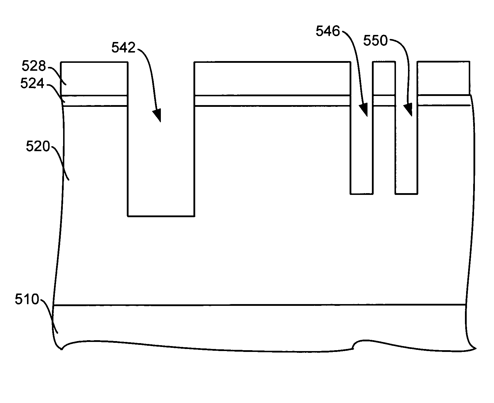
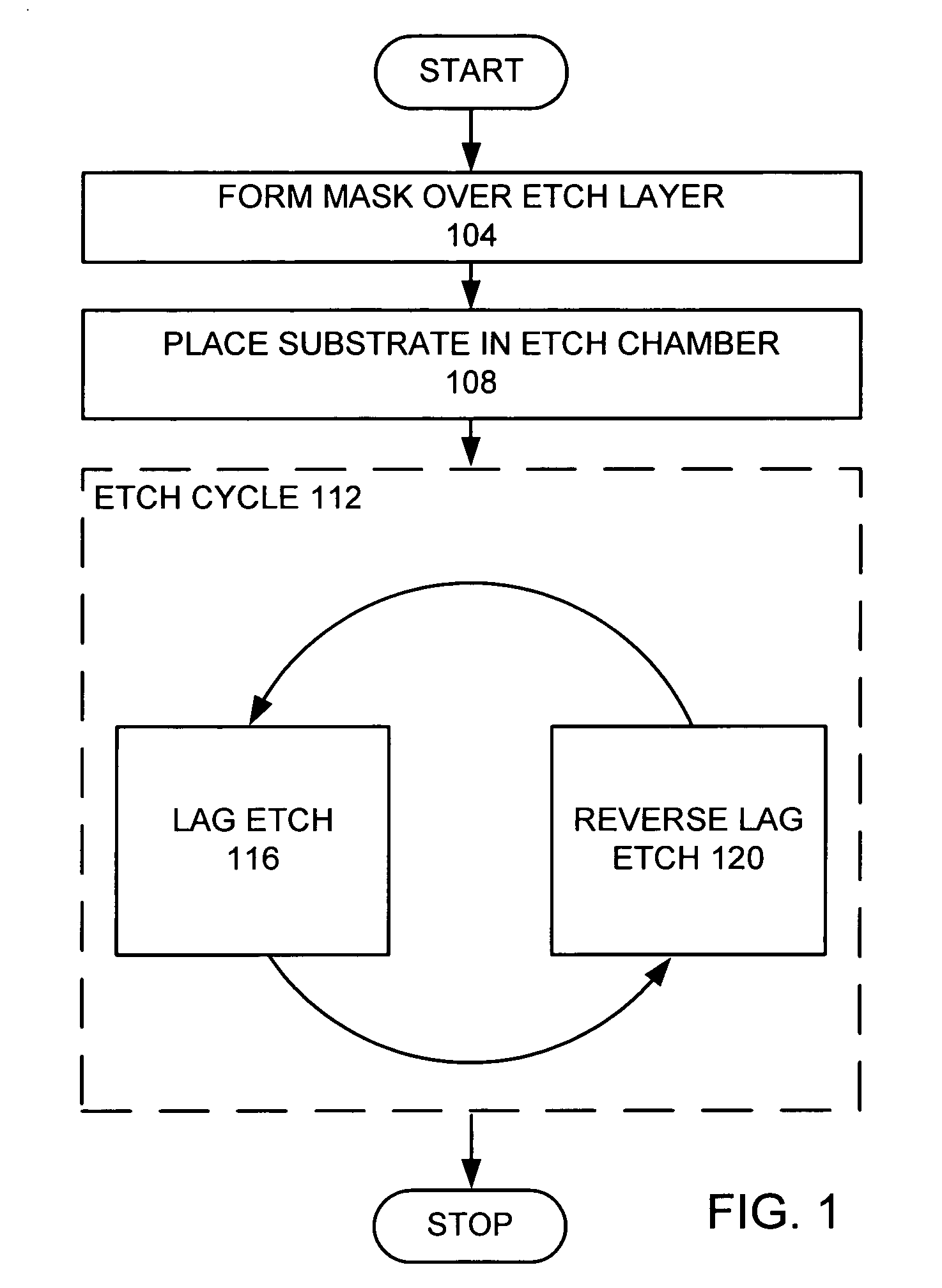
[0022]To facilitate understanding, FIG. 1 is a high level flow chart of a process used in an embodiment of the invention. A mask 528 is formed over an etch layer 520, which is disposed over a substrate 510 (step 104), as shown in FIG. 5A, which is a schematic cross-sectional view. Although this example shows that the etch layer 520 is contiguous to the substrate 510, one or more layers may...


PUM


Abstract

A method for etching features in a silicon oxide based dielectric layer over a substrate, comprising performing an etch cycle. A lag etch partially etching features in the silicon oxide based dielectric layer is performed, comprising providing a lag etchant gas, forming a plasma from the lag etchant gas, and etching the etch layer with the lag etchant gas, so that smaller features are etched slower than wider features. A reverse lag etch further etching the features in the silicon oxide based dielectric layer is performed comprising providing a reverse lag etchant gas, which is different from the lag etchant gas and is more polymerizing than the lag etchant gas, forming a plasma from the reverse lag etchant gas, and etching the silicon oxide based dielectric layer with the plasma formed from the reverse lag etchant gas, so that smaller features are etched faster than wider features.

Description

BACKGROUND OF THE INVENTION[0001]During semiconductor wafer processing, features of the semiconductor device are defined in the wafer using well-known patterning and etching processes. In these processes, a photoresist (PR) material may be deposited on the wafer and then is exposed to light filtered by a reticle. The reticle may be a transparent plate that is patterned with exemplary feature geometries that block light from propagating through the reticle.[0002]After passing through the reticle, the light contacts the surface of the photoresist material. The light changes the chemical composition of the photoresist material such that a developer can remove a portion of the photoresist material. In the case of positive photoresist materials, the exposed regions are removed, and in the case of negative photoresist materials, the unexposed regions are removed. Thereafter, the wafer is etched to remove the underlying material from the areas that are no longer protected by the photoresis...

Claims


Application Information

Patent Timeline
Patent Type & Authority Patents(United States)
IPC IPC(8): H01L21/302
CPCH01L21/31138H01L21/31116
Inventor WORSHAM, BINET A.KANG, SEAN S.WEI, DAVIDPOHRAY, VINAYYEN, BI MING
Owner LAM RES CORP
Why Eureka
Try Eureka