Electron emitter and method of producing the same

a technology of electron emitter and emitter, which is applied in the manufacture of electric discharge tube/lamp, discharge tube luminescnet screen, instruments, etc., can solve the problems of high production cost, inability to perform electron emission stably, and inability to meet the requirements of practical use of conventional electron emitters, etc., to achieve large polarization, improve electron emission efficiency, and reduce the effect of electron emission efficiency

Inactive Publication Date: 2007-12-11
NGK INSULATORS LTD
View PDF70 Cites 26 Cited by
  • Summary
  • Abstract
  • Description
  • Claims
  • Application Information

AI Technical Summary

Benefits of technology

[0017]In this case, if the polarization in the substance serving as the emitter is large, large polarization reversal occurs when the polarity of the drive voltage is reversed. Thus, the number of electrons emitted from the first or second electrode is large, and the number of electrons emitted from the substance serving as the emitter is large. That is, by simply providing the triple junction, it is possible to improve the electron emission efficiency of the electron emitter.
[0037]Further, it is preferable that the tip end of the outer peripheral portion is formed to have an acute shape at the time of providing the gap, since the electric field concentration occurs further intensely at the tip end, and the electrons are easily emitted from the tip end at the time of polarization reversal.

Problems solved by technology

All of these disclosed electron emitters are disadvantageous in that since no dielectric material is employed in the emitter section, a forming process or a micromachining process is required between facing electrodes, a high voltage needs to be applied between the electrodes to emit electrons, and a panel fabrication process is complex and entails a high production cost.
However, in the conventional electron emitters, the electron emission is not performed stably, and the number of emitted electrons is merely tens of thousands.
Therefore, conventional electron emitters are not suitable for practical use.
Advantages of an electron emitter having an emitter section made of a dielectric material have not been achieved.

Method used


Image

  • Electron emitter and method of producing the same
  • Electron emitter and method of producing the same
  • Electron emitter and method of producing the same

Examples


first embodiment

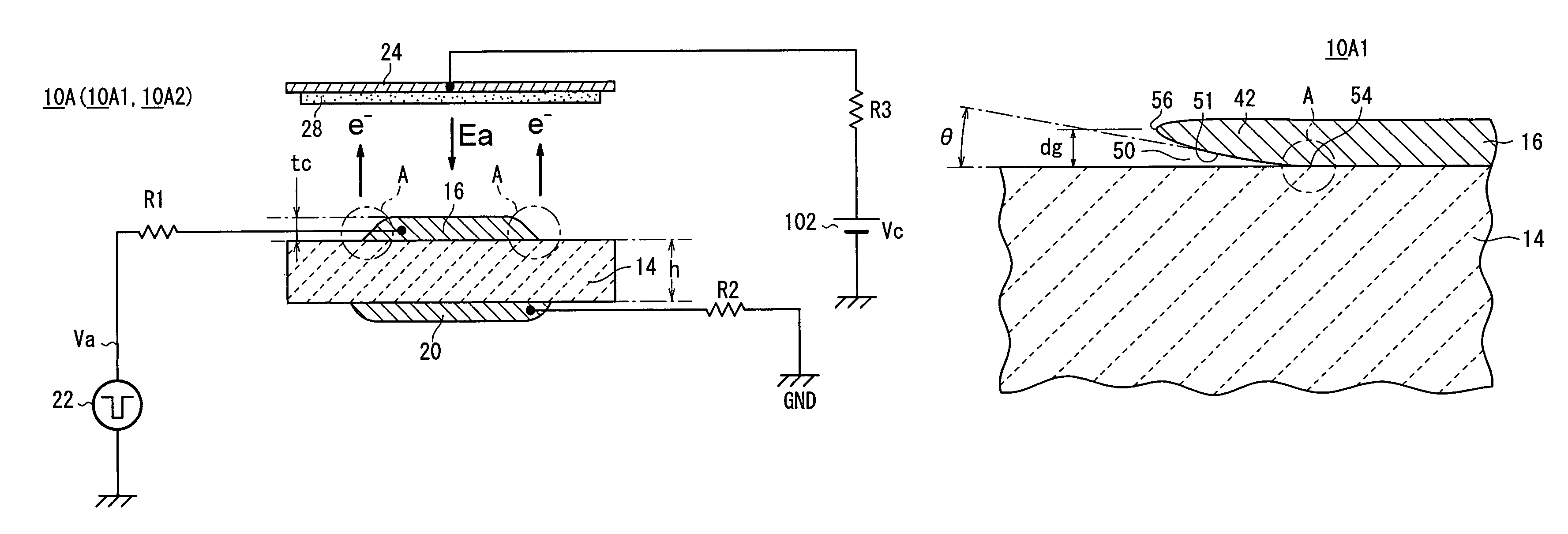
[0113]As shown in FIG. 1, an electron emitter 10A has an emitter section (substance serving as an emitter) 14 having a plate shape, a first electrode (cathode electrode) 16 formed on a front surface of the emitter section 14, a second electrode (anode electrode) 20 formed on a back surface of the emitter section 14, and a pulse generation source 22. A drive voltage Va from a pulse generation source 22 is applied between the cathode electrode 16 and the anode electrode 20 through a resistor R1.

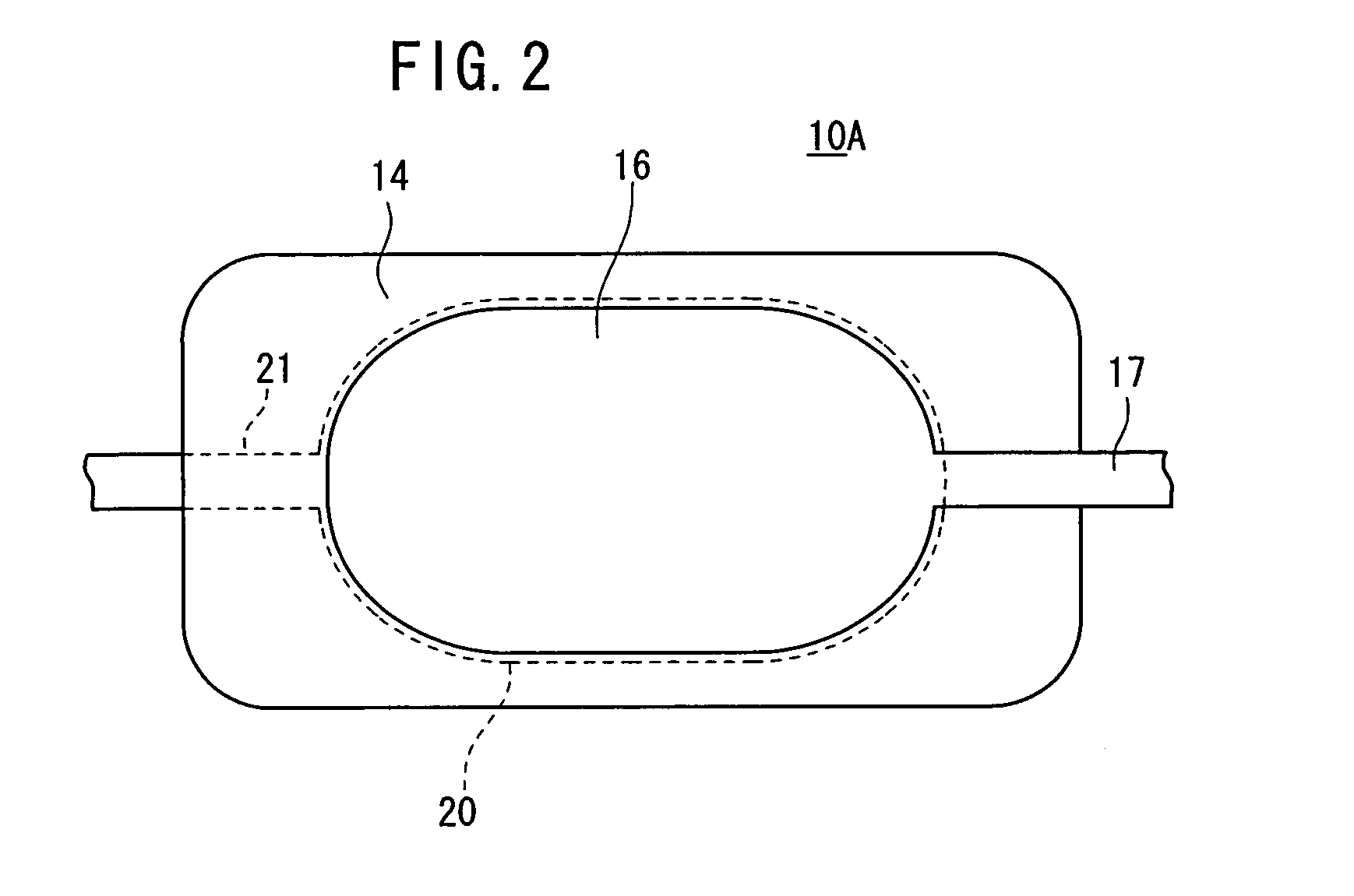
[0114]In an example shown in FIG. 1, the anode electrode 20 is connected to GND (ground) through a resistor R2 and hence set to a zero potential. However, the anode electrode 20 may be set to a potential other than the zero potential. As shown in FIG. 2, the drive voltage Va is applied between the cathode electrode 16 and the anode electrode 20 through a lead electrode 17 extending from the cathode electrode 16 and a lead electrode 21 extending from the anode electrode 20, for example.

[0115]Fo...

second embodiment

[0225]Next, an electron emitter 10B will be described.

[0226]The structure of the electron emitter 10B according to the second embodiment is substantially similar to the structure of the electron emitter 10A according to the first embodiment, however, differs in that a plurality of electron emitters 10(1), 10(2), 10(3) are formed on one substrate 12 as shown in FIG. 25.

[0227]That is, in the electron emitter 10B, anode electrodes 20a, 20b, 20c are independently formed on a surface of one substrate 12. Emitter sections 14a, 14b, 14c are formed on upper surfaces of the anode electrodes 20a, 20b, 20c, respectively. Further, cathode electrodes 16a, 16b, 16c are formed on the emitter sections 14a, 14b, 14c, respectively. The emitter sections 14a, 14b, 14c are interposed between the anode electrodes 20a, 20b, 20c, and the cathode electrodes 16a, 16b, 16c, respectively. Slits 80 are formed between the electron emitter 10(1) and the electron emitter 10(2), and between the electron emitter 10...

third embodiment

[0258]Next, an electron emitter 10C will be described with reference to FIG. 30.

[0259]As shown in FIG. 30, the structure of the electron emitter 10C according to the third embodiment 10C is substantially similar to the structure of the electron emitter 10A according to the first embodiment, however, differs in that the electron emitter 10C has one substrate 110 made of, e.g., ceramics, the anode electrode 20 is formed on the surface of the substrate 110, the emitter section 14 is formed on the substrate 110 to cover the anode electrode 20, and the cathode electrode 16 is formed on the emitter section 14.

[0260]A space 112 is formed in the substrate 110 at a position for forming each emitter section 14. The space 112 forms a thin wall section as described later. The space 112 is connected to the outside through a small diameter through hole 114 provided on the other surface of the substrate 110.

[0261]The substrate 110 has a thin region where the space 112 is formed. The thin region i...


PUM


Abstract

An electron emitter includes an emitter section having a plate shape, a cathode electrode formed on a front surface of the emitter section, and an anode electrode formed on a back surface of the emitter section. A gap is formed between an outer peripheral portion of the cathode electrode and the front surface of the emitter section. The front surface of the emitter section contacts a lower surface of the outer peripheral portion to form a base end as a triple junction. The gap expands from the base end toward a tip end of the outer peripheral portion.

Description

[0001]This application claims the benefit of Japanese Application 2003-346091, filed Oct. 3, 2003, the entirety of which is incorporated herein by reference.BACKGROUND OF THE INVENTION[0002]1. Field of the Invention[0003]The present invention relates to an electron emitter including a first electrode and a second electrode formed on a substance serving as an emitter. Further, the present invention relates to a method of producing the electron emitter.[0004]2. Description of the Related Art[0005]In recent years, electron emitters having a cathode electrode and an anode electrode have been used in applications such as field emission displays (FEDs) and backlight units. In an FED, a plurality of electron emitters are arranged in a two-dimensional array, and a plurality of phosphors are positioned at predetermined intervals in association with the respective electron emitters.[0006]Conventional electron emitters are disclosed in Japanese laid-open patent publication No. 1-311533, Japane...

Claims


Application Information

Patent Timeline
Patent Type & Authority Patents(United States)
IPC IPC(8): G01G3/10H01J29/70H01J9/02G09G3/10H01J1/02H01J1/14H01J1/30H01J1/304H01J1/312H01J1/32H01J3/02
CPCB82Y10/00H01J9/022H01J1/32H01J1/312
Inventor TAKEUCHI, YUKIHISANANATAKI, TSUTOMUOHWADA, IWAO
Owner NGK INSULATORS LTD
Why Eureka
Try Eureka