Semiconductor device and method of fabricating the same

a technology of semiconductor devices and semiconductors, applied in semiconductor devices, electrical devices, transistors, etc., can solve problems such as data read errors, data leakage, data loss, etc., and achieve the effect of minimizing the structure of the sonos cell without degrading the programming and read performan

Active Publication Date: 2007-12-18
INFINEON TECH LLC
View PDF9 Cites 0 Cited by
  • Summary
  • Abstract
  • Description
  • Claims
  • Application Information

AI Technical Summary

Benefits of technology

[0019]The present invention has been made taking the above problems into consideration, and has an object of providing a semiconductor device capable of normally programming each bit in the same cell without being affected by the amounts of charges in the other bit or bits and further miniaturizing the SONOS cell structure without degrading the programming and read performance, and a method of manufacturing such a semiconductor device.
[0020]According to an aspect of the present invention, there is provided a semiconductor device including: a substrate having a pair of first diffused regions; and a gate including an oxide film provided on the substrate, and a charge storage layer provided on the oxide film, the charge storage layer being an electrical insulator capable of storing charges in bit areas, the oxide film having first portions related to the bit areas and a second portion that is located between the bit areas and is thicker than the first potions, the first portions serving as tunneling oxide portions, while the second portion allows reduced tunneling.
[0028]According to another aspect of the present invention, there is provided a method of fabricating a semiconductor device comprising the steps of: (a) forming a tunneling oxide film having a uniform thickness on a substrate; (b) forming a pair of first diffused regions in the substrate; (c) forming a surface protection film provided on the tunneling oxide film and located above the pair of first diffused regions; and (d) re-oxidizing the tunneling oxide film exposed through the surface protection film so that the tunneling oxide film has a self-aligned portion having a thickness that allows reduced tunneling of charges.

Problems solved by technology

The floating gate structure has a disadvantage in that the charge may leak because of the use of the conductive polysilicon for storing the charge, and data may be lost.
This may cause a data read error.

Method used


Image

  • Semiconductor device and method of fabricating the same
  • Semiconductor device and method of fabricating the same
  • Semiconductor device and method of fabricating the same

Examples


first embodiment

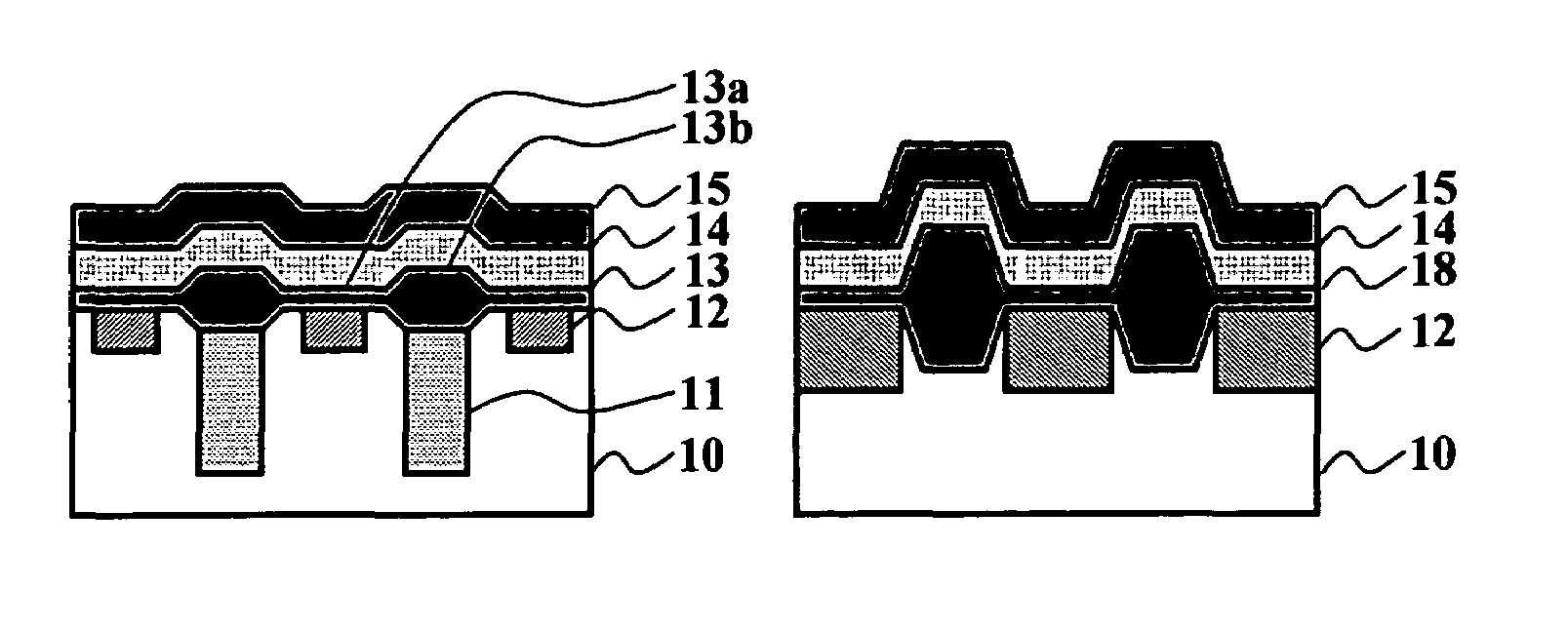
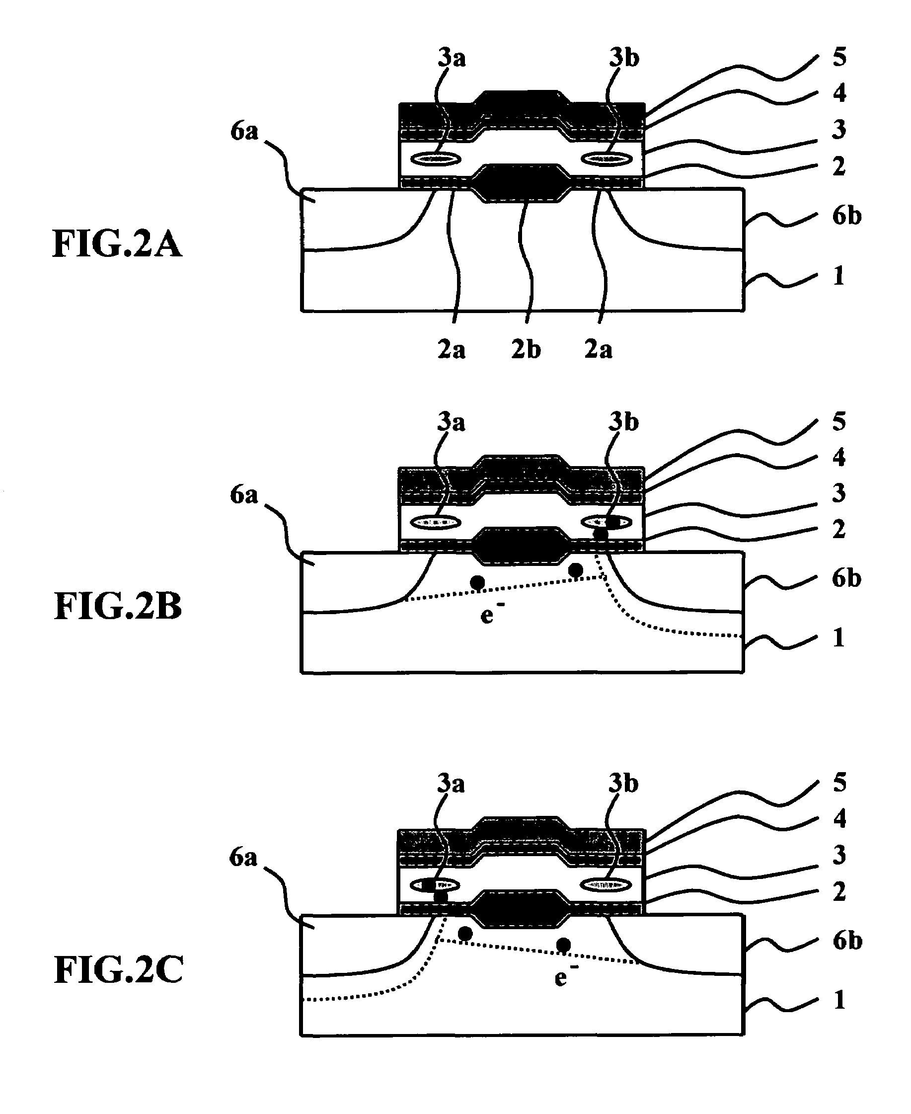
[0064]FIGS. 3A and 3B are respectively cross-sectional views of a cell having a first exemplary structure of the semiconductor device of the present invention that has the gate of the SONOS structure and the buried bit line structure. More particularly, FIG. 3A shows the core area, and FIG. 3B shows the cell peripheral area. In the core area, a plurality of cells are arrayed, and each of which cells has the fundamental structure shown in FIG. 2A, and operates as has been described with reference to FIGS. 2B and 2C.

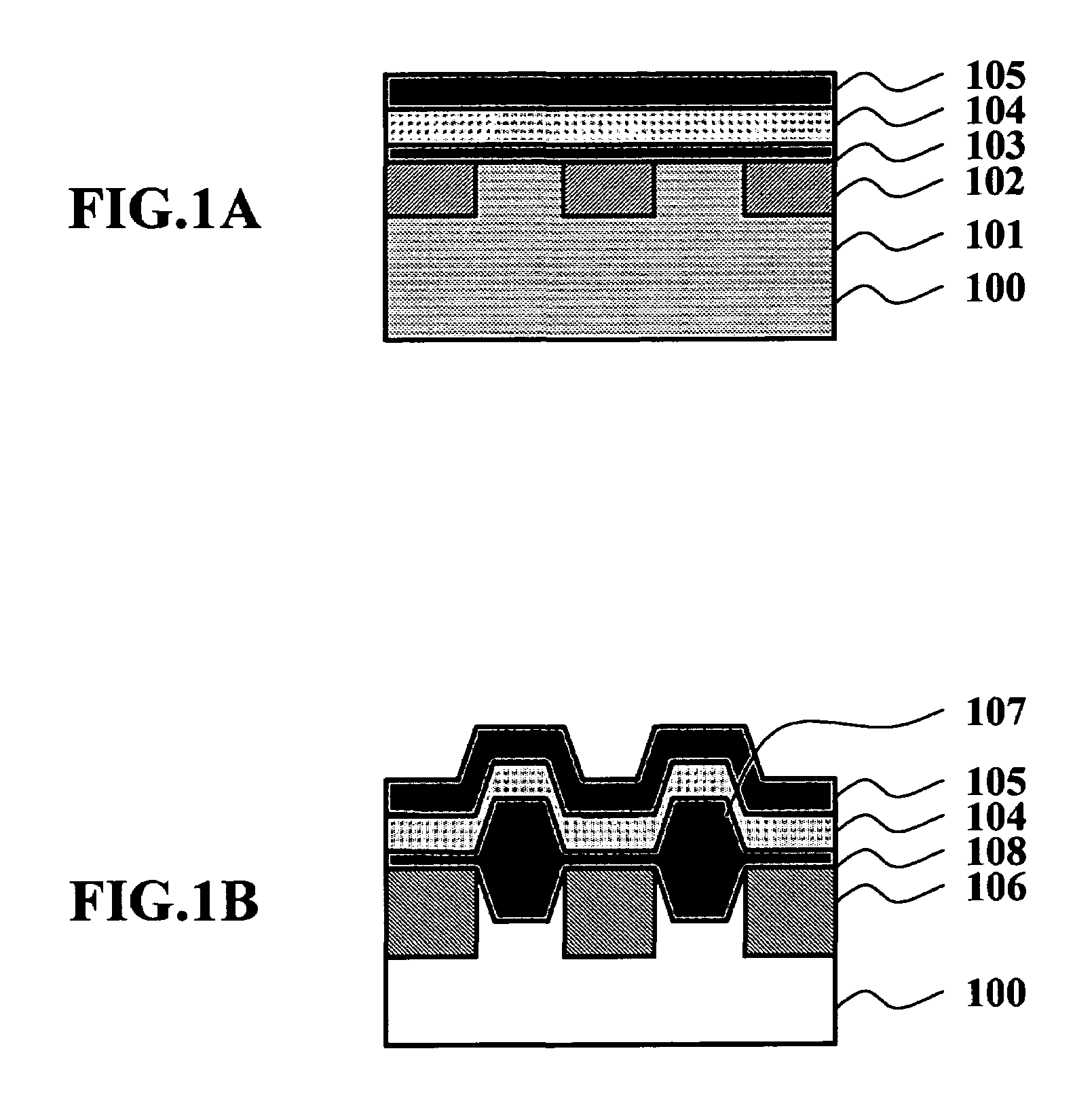
[0065]FIGS. 4A through 6I are views for describing the process of fabricating the present semiconductor device, in which the left-side figures show the core area, and the right-side figures show the peripheral area.

[0066]In the core area, the n-type diffused regions 12 for the bit lines are formed, at equal intervals, on the main surface of the p-type semiconductor substrate 10 through As implantation. Each of the n-type diffused regions 12 functions as the source / drain re...

second embodiment

[0078]FIGS. 7A and 7B are respectively cross-sectional views of the cell having a second exemplary structure of the semiconductor device of the present invention. More particularly, FIG. 7A shows the core area, and FIG. 7B shows the cell peripheral area. FIGS. 8A through 8C show the process of fabricating the present semiconductor device, wherein the left-side figures show the core area and the right-side figures show the cell peripheral area.

[0079]The structure of the cell peripheral area of the semiconductor device is the same as that of the first exemplary structure shown in FIG. 3B. The structure of the core area shown in FIG. 7A differs from that of the first exemplary structure shown in FIG. 3A in that the first structure has the ion-implanted region 11 for the adjustment of the threshold values applied to the whole surface of the semiconductor substrate 10, while the second structure has the ion-implanted regions 11 applied only to the channel regions located between the n-ty...

third embodiment

[0088]The semiconductor device of the present embodiment has a structure similar to that shown in FIGS. 7A and 7B, but has a process for forming the n-type diffused regions different from that employed in the second embodiment.

[0089]FIGS. 9A through 9D describe the process of forming the n-type diffused regions of the present invention, wherein the left-side figures show the core area and the right-side figures.

[0090]The thin oxide film (having a thickness of approximately 7 nm) is uniformly formed on the main surface of the semiconductor substrate 10, and the polysilicon film 19 is deposited on the oxide film 18. Then, the polysilicon film 19 is partially etched by the photolithographic process to form openings arranged at given intervals (FIG. 9A).

[0091]Next, a nitride film is uniformly deposited and is etched to form nitride sidewall films 23 on opposite sides of the patterned polysilicon films 19 arranged on the thin oxide film 18 at given intervals. After that, As ions are impl...


PUM


Abstract

A semiconductor device includes a substrate having a pair of first diffused regions, and a gate including an oxide film provided on the substrate, and a charge storage layer provided on the oxide film, the charge storage layer being an electrical insulator capable of storing charges in bit areas. The oxide film has first portions related to the bit areas and a second portion that is located between the bit areas and is thicker than the first potions. The first portions serve as tunneling oxide portions, while the second portion allows reduced tunneling.

Description

CROSS REFERENCE TO RELATED APPLICATION[0001]This is a continuation of International Application No. PCT / JP2004 / 008319, filed Jun. 14, 2004.BACKGROUND OF THE INVENTION[0002]1. Field of the Invention[0003]The present invention relates to a semiconductor device and a method of fabricating the same, and more particularly, to a read only or programmable non-volatile semiconductor device capable of storing charges in a gate insulation film and a method of fabricating the same.[0004]2. Description of the Related Art[0005]The semiconductor memories are categorized into a volatile type in which information is lost by power off and a non-volatile type in which information is retained even by power off. A typical-example of the latter non-volatile memory is a flash memory capable of erasing all data in an area at once, so that the rewriting time can be reduced.[0006]Recently, there has been proposed a multi-bit cell structure, which may have has a MNOS (Metal (gate)-Nitride-Oxide-Silicon) stru...

Claims


Application Information

Patent Timeline
Patent Type & Authority Patents(United States)
IPC IPC(8): H01L29/788H01L21/336H01L21/8246H01L21/8247H01L27/115H01L29/792
CPCH01L27/115H01L27/11526H01L27/11534H01L27/11568H01L29/7923H01L29/42368H01L29/66833H01L29/7887H01L29/1037H10B41/40H10B41/43H10B43/30H10B69/00
Inventor OKANISHI, MASATOMI
Owner INFINEON TECH LLC
Why Eureka
Try Eureka