
Contactor for electronic components and test method using the same

a technology of electronic components and contactors, which is applied in the direction of individual semiconductor device testing, coupling device connection, instruments, etc., can solve the problems of inability to perform parallel pushing, inability to obtain contact stability, and complicated contact pins provided in the contactors, etc., to achieve easy replacement of contact electrodes and ease of replacemen

Inactive Publication Date: 2007-12-18
SOCIONEXT INC
View PDF4 Cites 9 Cited by
  • Summary
  • Abstract
  • Description
  • Claims
  • Application Information

AI Technical Summary

Benefits of technology

[0030]Accordingly, it is a general object of the present invention to provide a contactor in which the above-described disadvantages are eliminated, and a test method using the contactor.
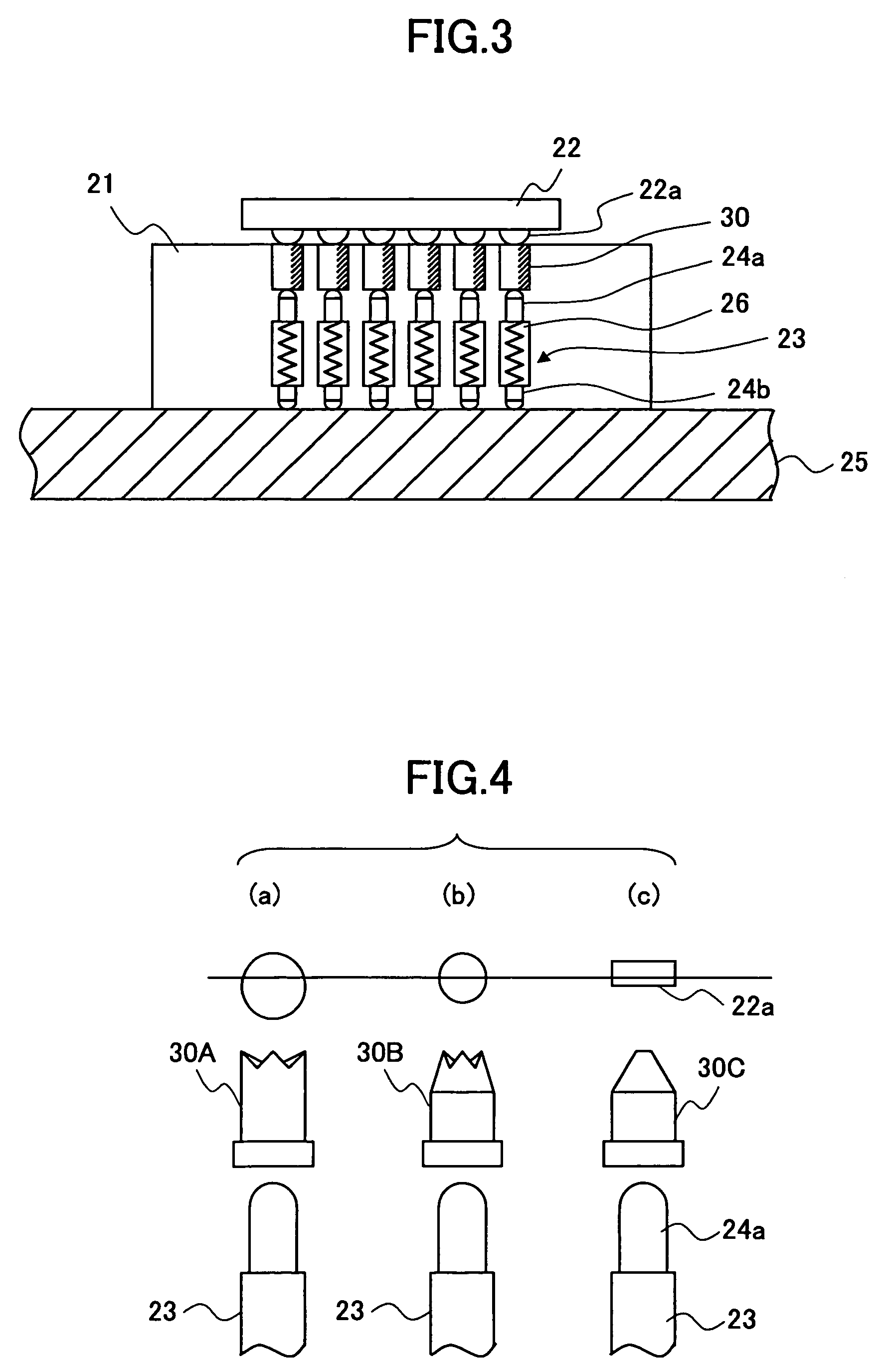
[0031]A more specific object of the present invention is to provide a contactor having contact electrodes that are easy to change in size and shape in accordance with the size and shape of the external terminals of an IC package to be contacted.
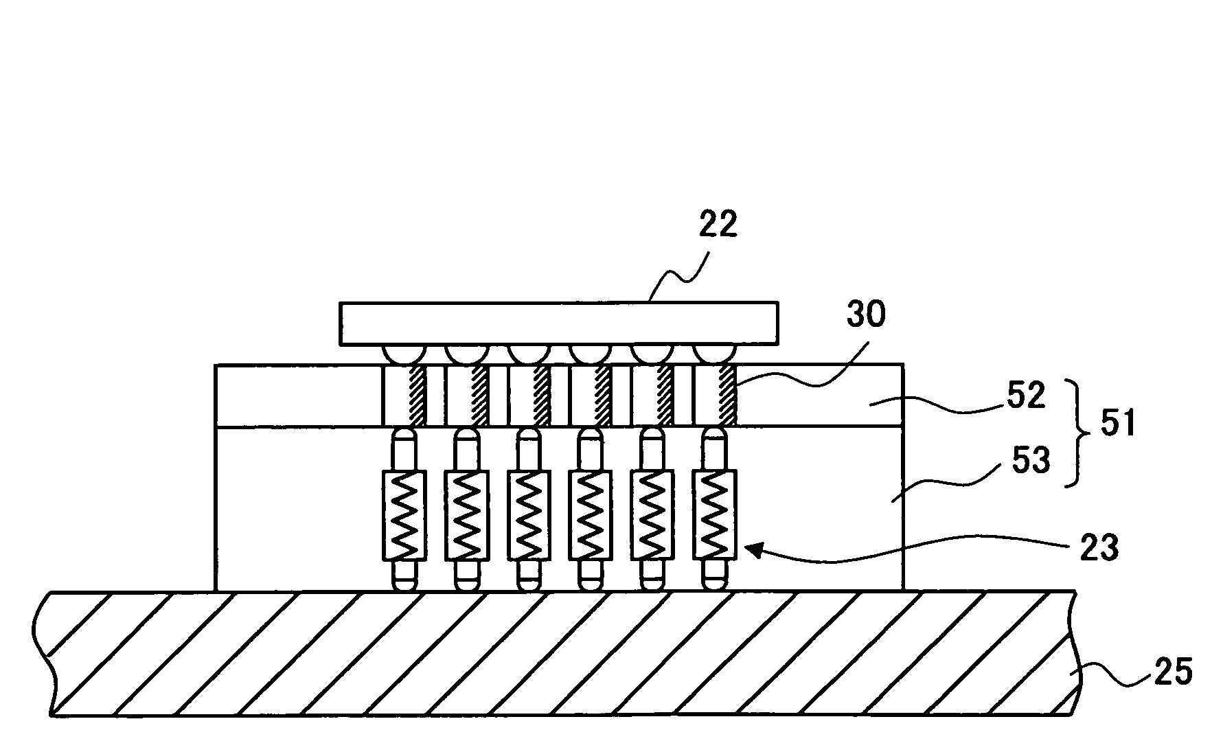
[0036]Thus, according to the present invention, a contactor that can easily have the size and shape of contact electrodes changed in accordance with the size and shape of the external electrodes of an IC package or IC chip to be contacted can be realized.
[0037]Further, according to the present invention, the contact electrodes are separable from the elastic electrodes. Therefore, it is possible to replace the contact electrodes with ease. Accordingly, it is possible to replace only the contact electrodes in accordance with the shape and size of the external electrodes of an electronic component. As a result, there is no need to replace the entire contactor. Further, there is no need to prepare multiple types of contactors for the external electrodes of various types of electronic components. Since it is possible to separate and detach only a contact electrode holding part holding the contact electrodes, it is possible to replace only the contact electrodes with new or cleaned ones with ease.
[0038]Further, according to the present invention, if the contact electrodes are worn out or broken or a foreign material is attached to the contact electrodes in the case of bringing a contactor into contact with the terminals of a test circuit board, the contact electrodes are easily replaced. Further, when spring electrodes buckle at the time of contact, contact with the external terminals of an IC package or IC chip can be made with accuracy. Likewise, contact with the terminals of the test circuit board can be made with accuracy. Further, it is possible to bring the contactor into contact with the test circuit board without damaging the terminals of the test circuit board.

Problems solved by technology

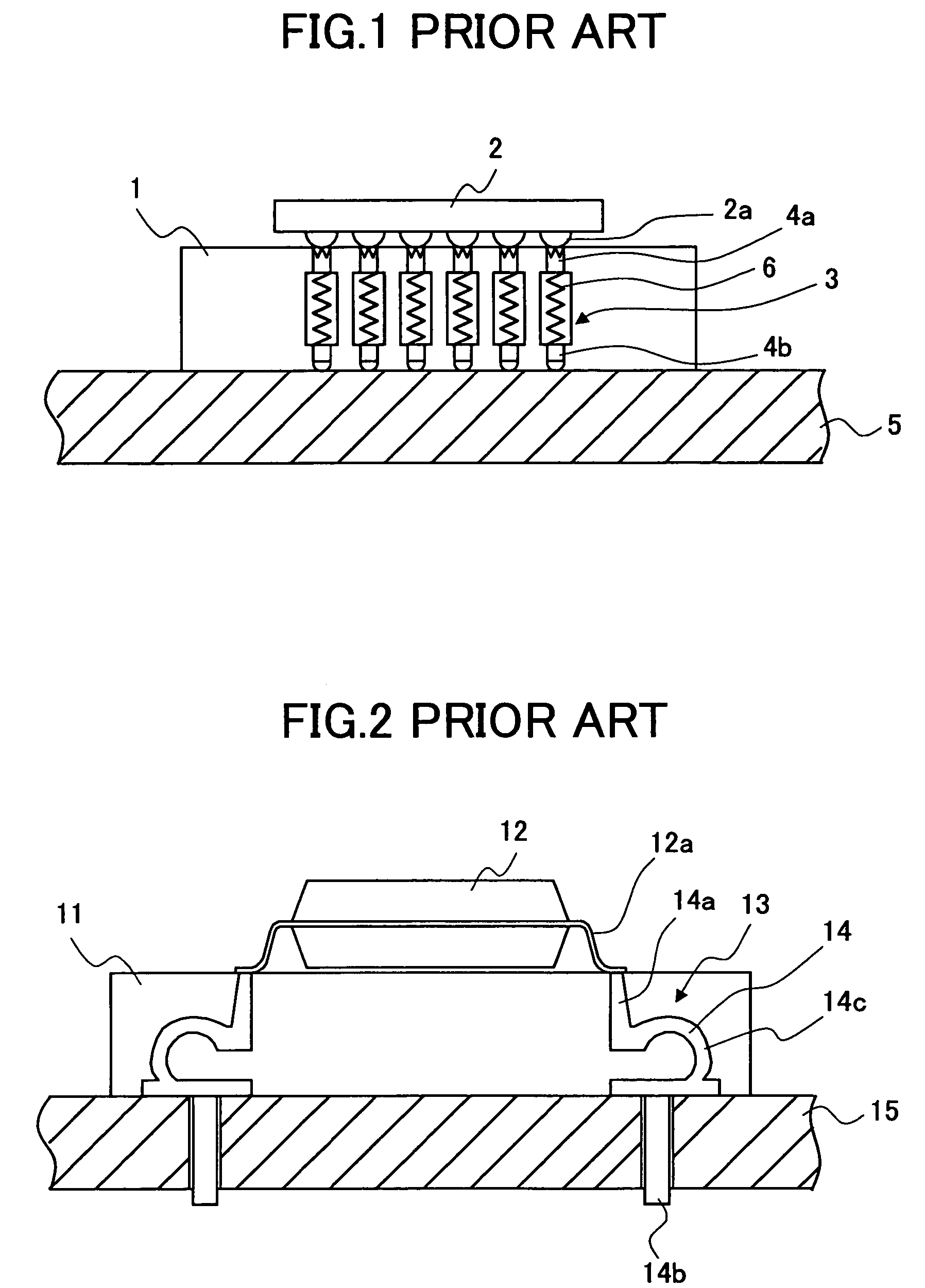
Accordingly, contact pins provided in the contactors are required to be more complicated and minute in shape.
When an IC package is pushed into such a contactor as described above to be mounted thereon using an automatic machine such as a test handler in a mass production process, “parallel pushing” may not be performable depending on factors such as parallelism on the automatic machine side, board parallelism, and board deflection.
Accordingly, since contact pins normally show their optimum spring characteristics when they are pushed straight, a normal operating state cannot be obtained, so that contact stability cannot be obtained.
Further, springs provided in the contactor are likely to have a shortened useful service life.
Particularly, the deposition of transferred solder plating on the contact parts of the contact pins causes a problem.
That is, the surface of the solder plating transferred to the contact parts is oxidized into an insulating foreign material, thus resulting in poor contact.
Further, the deposition of foreign material such as dust in a laboratory or the residual resin of an IC package on the contact parts of the contact pins also results in poor contact.
External terminals using lead-free solder, for which there have been increasing demands for environmental reasons, do not permit attachment or mixture of lead in light of the reasons for the demands.
Further, when a problem occurs in a BGA-type IC package after the IC package is once mounted on a board, an electrical test should be conducted on the IC package after the IC package is removed from the board.
This operation of providing solder balls requires a lot of time and effort.
The same problems as described above, that is, unstable contact in the case where “parallel pushing” is not performable and a shortened useful service life of springs, are likely to occur between contact electrodes on the test circuit board side and the terminals of a test circuit board.
The contact with the terminals of the board is likely to cause damage such as concave scratches and plating peeling to the contactor.
This often results in poor contact.
The above-described problems such as unstable contact in the case where “parallel pushing” is not performable, a shortened useful service life of springs, the transfer of chip outer plating and resultant poor contact, and the attachment of lead solder to and the mixture of lead solder into a lead-free product also occur in IC chips.
Accordingly, contact deficiency and damage to a terminal of a circuit board are likely to occur at the time of contact.
Further, since contact displacement is limited, unstable contact in the case where “parallel pushing” is not performable is likely to occur.
Further, the material of the contact pins is not freely selectable since priority is given to the spring characteristic of the contact pins.
Furthermore, since the contact pins are formed from a plate material by etching or molding, their end shape, or contact electrode shape, is not freely selectable.
For the reasons stated above, the above-described problems are likely to occur.

Method used


Image

  • Contactor for electronic components and test method using the same
  • Contactor for electronic components and test method using the same
  • Contactor for electronic components and test method using the same

Examples


third embodiment

[0095]Further, as in the above-described third embodiment, when foreign material is attached to the contact part of the contact electrode 30, the foreign material can be easily removed after detaching the contact electrode holding part 72. At this point, the detached contact electrode holding part 72 may be returned to where it was immediately after the foreign material is removed therefrom by cleaning. Alternatively, the detached contact electrode holding part 72 may be replaced with another clean contact electrode holding part 72. As a result, it is possible to remove the foreign material from the detached contact electrode holding part 72 in a separate process while continuing a test. Accordingly, the test process can be continued without being affected by the attachment of the foreign material.

[0096]Next, a description is given, with reference to FIG. 13, of a variation of the fourth embodiment. FIG. 13 is a sectional view of a contactor 81 according to the variation of the four...

seventh embodiment

[0125]The configuration of this embodiment is equal in the other aspects to that of the seventh embodiment and a description thereof is omitted.

[0126]In the above-described embodiments, as a contact electrode material, a metal material such as steel (an SK steel) or copper alloy as a conductive material is preferably used. Surface treatment may be applied on the contact part of the contact electrode. For instance, the contact part of the contact electrode may be plated with a platinum metal such as rhodium or palladium, to which solder is less likely to be transferred, or an alloy of such platinum metals. Further, the contact part of the contact electrode may be plated with metal having high hardness so as to prevent wear of the contact part. Further, in the case of alloy materials composed of sliver, platinum, copper, gold, and palladium, no surface plating is necessary. Even if the surface of the contact part is further polished, the surface is prevented from being oxidized, so th...


PUM


Abstract

A contactor configured to be electrically connected to the terminals of an electronic component is disclosed. The connector includes multiple contact electrodes contacting the terminals of the electronic component and multiple elastic electrodes each composed of an electrically conductive elastic body. The elastic electrodes generate a pressing force for pressing the contact electrodes against the terminals of the electronic component. The contact electrodes are separable from the elastic electrodes.

Description

CROSS-REFERENCE TO RELATED APPLICATION[0001]The present application is based on Japanese Priority Patent Applications No. 2003-154678, filed on May 30, 2003, and No. 2004-125850, filed on Apr. 21, 2004, the entire contents of which are hereby incorporated by reference.BACKGROUND OF THE INVENTION[0002]1. Field of the Invention[0003]The present invention relates to a contactor employed to test the characteristics of electronic components such as semiconductor integrated circuits, and a test method using the contactor.[0004]2. Description of the Related Art[0005]In recent years, there have been increasing demands for reduction in the size and weight of electronic apparatuses such as personal digital assistants (PDAs), cellular phones, and digital cameras. This has also caused strong demands for reduction in the size and weight of electronic components used in these electronic apparatuses, such as semiconductor integrated circuits.[0006]These demands are met by a rapid increase in semic...

Claims


Application Information

Patent Timeline
IPC IPC(8): G01R31/02G01R1/04G01R1/06G01R31/26G01R1/067G01R1/073H01R33/76
CPCG01R1/0483G01R1/0441
Inventor TASHIRO, KAZUHIROMARUYAMA, SHIGEYUKIKOIZUMI, DAISUKEKUMATABARA, TAKUMIFUKUDA, KEISUKE
Owner SOCIONEXT INC
Learn More