

Magnetic memory device
a magnetic memory and random access technology, applied in information storage, static storage, digital storage, etc., can solve the problems of high anisotropy energy, high energy consumption, and reduced available energy (ksub>u/sub>v) for storing bit messages, etc., to achieve high heat tolerance during thermal assistant writing, low power dissipation, and high thermal stability
- Summary
- Abstract
- Description
- Claims
- Application Information
AI Technical Summary
Benefits of technology
Problems solved by technology
Method used
Image

Examples
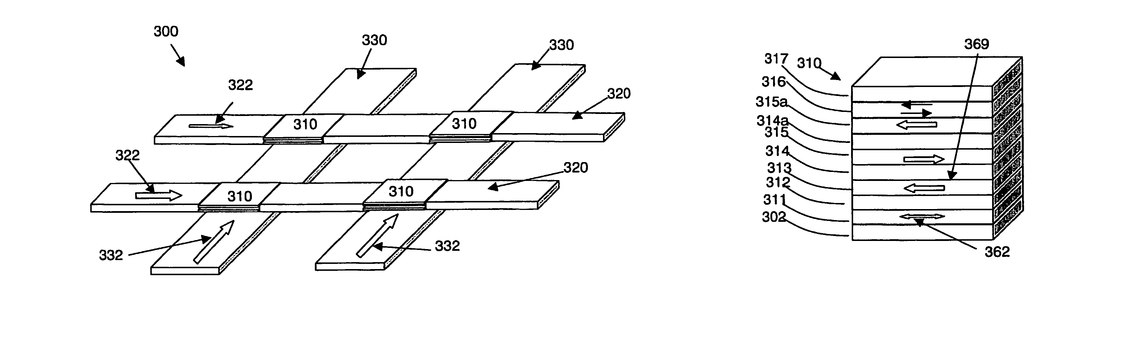
first embodiment
[0052]Referring now to FIGS. 5A and 5B, the writing operation of magnetization states in a CIP SV MRAM unit in accordance with the present invention is shown.
[0053]In FIG. 5A there is shown a memory cell 501 which is already described in detail in FIG. 3B as memory cell 310, a bit line 502 and a word line 503. The memory cell 501 is heated by current 515 present along the bit line 502. In a typical MRAM unit, the memory cell 501 is formed on a substrate (not shown) of the MRAM unit. The bit line 502 and the word line 503, which are electrically conductive layers, are also formed on the substrate.
[0054]Referring to FIG. 5A, in operation, the memory cell 501 is heated by applying a current 515 through the memory cell 501 along the bit line 502. When the temperature of the recording layer approaches or exceeds the critical temperature (the critical temperature being the blocking temperature of the AFM layer or being the Curie temperature of the hard magnetic layer, respectively, in the...
second embodiment
[0058]Referring now to FIGS. 7A and 7B, a CPP type MRAM structure according to the present invention is shown, similar to the CIP structure in FIGS. 6A and 6B. In FIG. 7A, the CPP (MTJ or CPP SV) MRAM structure comprises a CPP memory cell 723 which is already described in detail in FIG. 4B as memory cell 410, a bit line 722 and a word line 724. An initial heating current 725 is applied to the CPP memory cell 723 by the bit line 722 and the word line 724.
[0059]The writing operation of a CPP memory cell 723 in a MRAM is similar to the writing operation of the CIP memory cell 501 described earlier with respect to FIG. 5B. FIG. 7B illustrates the memory cell's writing operation wherein currents 726, 727 are applied along the bit line 722 and the word line 724, respectively, after the memory cell 723 is heated by an initial heating current 725.
[0060]In a fourth embodiment of the present invention, a CPP MRAM is shown in FIG. 8A, wherein a heat element 828 is provided under the memory cel...
PUM
 Abstract
Description
Claims
Application Information