

Highly-oriented diamond film, method for manufacturing the same, and electronic device having highly-oriented diamond film
a diamond film, high-oriented technology, applied in the direction of water-setting substance layered products, natural mineral layered products, transportation and packaging, etc., can solve the problems of unresolved problems, unusable device movement, and inability to form 50 m or less, and achieve the effect of substantially constant crystal grain size of diamond layer
- Summary
- Abstract
- Description
- Claims
- Application Information
AI Technical Summary
Benefits of technology
Problems solved by technology
Method used
Image

Examples
example
[0056]The advantageous effects of the present invention will now be described with reference to Examples in comparison with Comparative Examples which are out of the scope of the present invention.
[0057]First Test
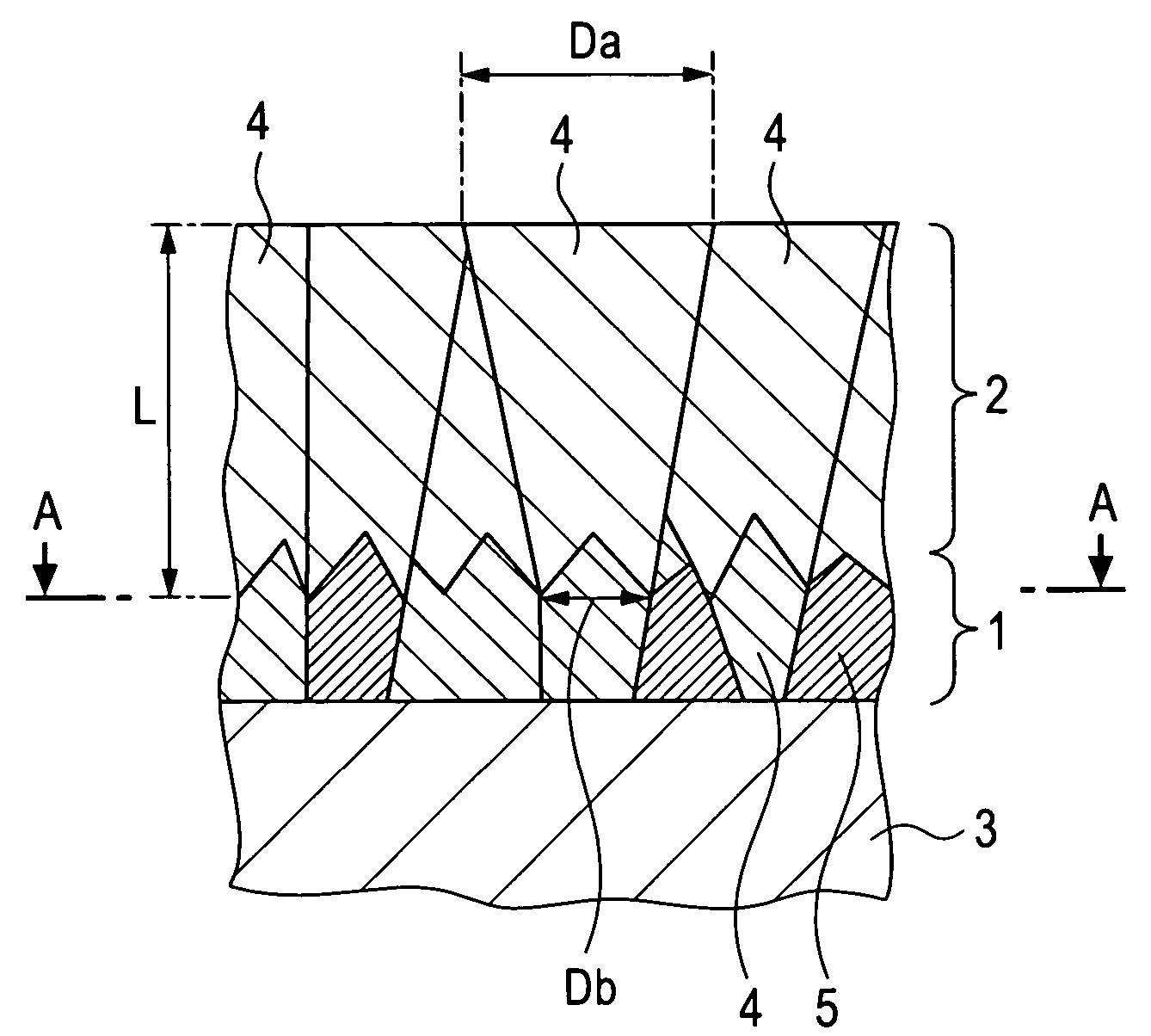
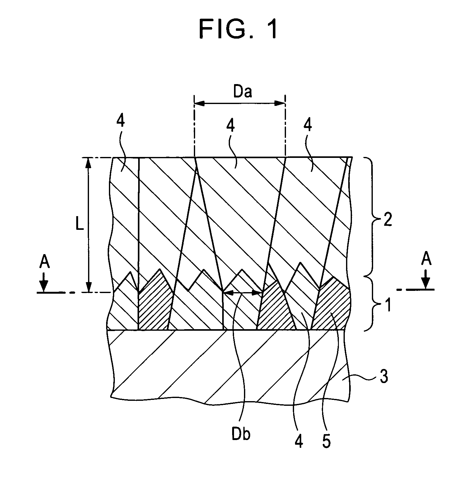
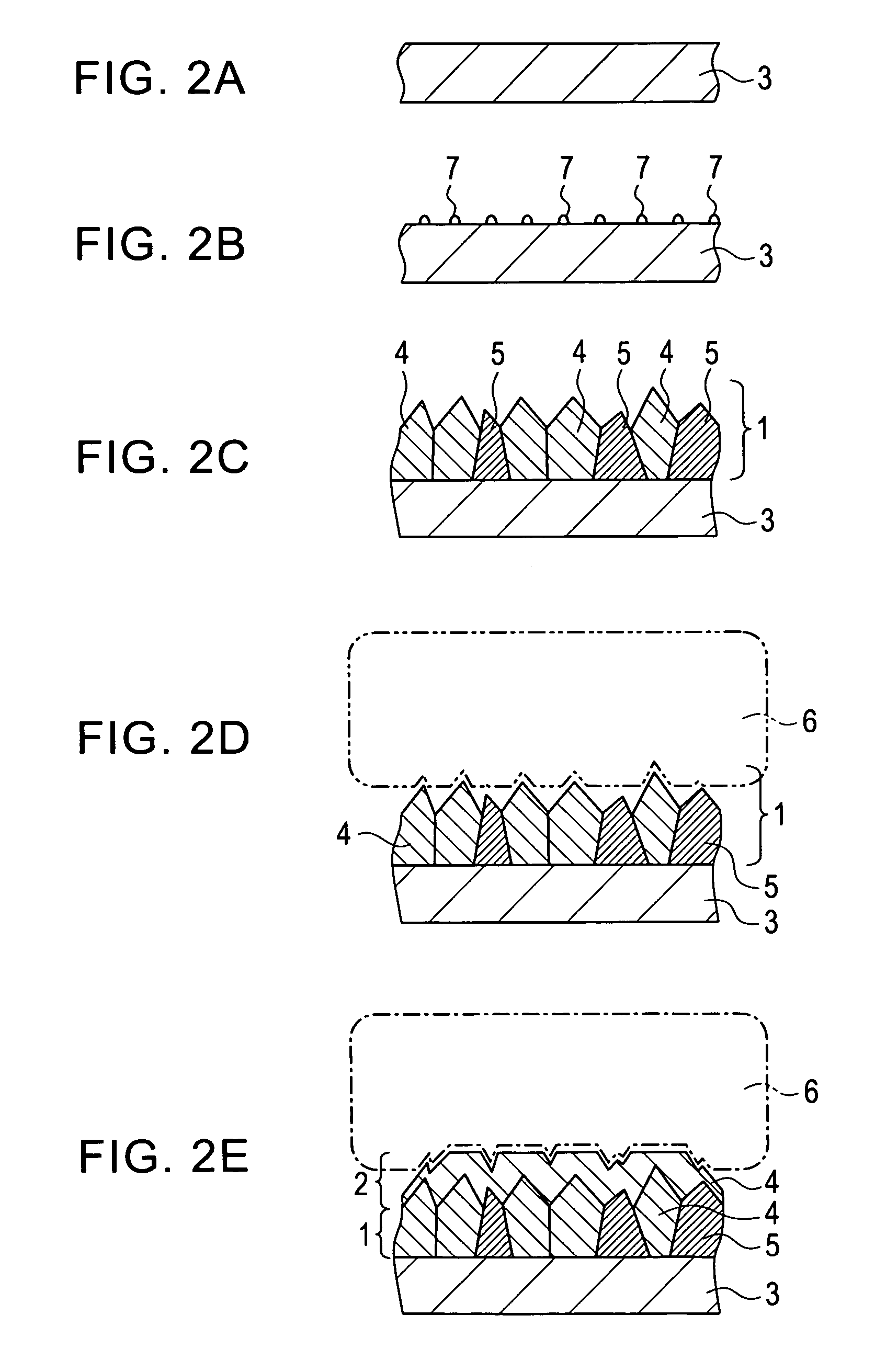
[0058]Firstly, the results of a first test will be described. A silicon substrate having a surface constituted by (100) planes was placed in a microwave CVD system and was irradiated with microwaves at a substrate temperature of 650° C. for 15 mins under a flow of a gaseous mixture of 2% methane by volume and 98% hydrogen by volume under conditions with a pressure of 33 hPa and a flow rate of 300 standard cm3 / min (sccm). At this time, the microwave input power was about 1 kW and then was slightly controlled so as to maintain the substrate temperature at 650° C. Simultaneously, a negative bias voltage was applied to the silicon substrate so that a current of 10 mA / cm2 flows. Thus, oriented diamond nuclei were formed on the surface of the silicon substrate.
[0059]Then, a diamo...
PUM
| Property | Measurement | Unit |
|---|---|---|
| average crystal grain size | aaaaa | aaaaa |
| average crystal grain size | aaaaa | aaaaa |
| crystal grain size | aaaaa | aaaaa |
Abstract
Description
Claims
Application Information