Holographic reticle and patterning method

a holographic reticle and patterning technology, applied in the field of semiconductor device lithography, can solve the problems of difficult inspection and repair of reticle b>10/b> defects, time-consuming tasks, and reticle defects, and achieve the effects of reducing the need for repair of defects, cost saving, and prolonging the lithography process window

Inactive Publication Date: 2007-12-25
TAIWAN SEMICON MFG CO LTD
View PDF15 Cites 3 Cited by
  • Summary
  • Abstract
  • Description
  • Claims
  • Application Information

AI Technical Summary

Benefits of technology

[0018]An advantage of preferred embodiments of the present invention includes providing a defect-withstanding reticle for patterning a target. Defects on the hologram reticle do not result in the formation of defects on the patterned target surface. Thus, there is a reduced need for repair of defects on the reticle, resulting in a cost savings. The depth of focus (DOF) may be increased to extend the lithography process window, particularly on a topographic substrate. A further advantage of preferred embodiments of the present invention is the ability to precisely control and decrease the DOF, and form three-dimensional (3-D) structures in the photoresist layer on the target.

Problems solved by technology

A disadvantage of prior art lithography is that this one-to-one relationship between the reticle 10 and the wafer 20 can result in a reticle defect 18, particularly if the defect is large, inducing a flaw 23a on a wafer 20.
Hard defects and / or soft defects can be formed during the manufacturing process or handling of a reticle 10.
Because reticles 10 are typically expensive and time-consuming to manufacture, attempts are usually made to repair them, rather than scrapping them.
However, reticle 10 defect inspection and repair are difficult, time-consuming tasks.
Also, laser repair of a reticle 10 can damage the reticle substrate, leaving a laser burn and possibly creating a printable defect on the substrate 21.
The repair of some reticle 10 defects is often impossible to achieve.

Method used


Image

  • Holographic reticle and patterning method
  • Holographic reticle and patterning method
  • Holographic reticle and patterning method

Examples


Embodiment Construction

[0050]The making and using of the presently preferred embodiments are discussed in detail below. It should be appreciated, however, that the present invention provides many applicable inventive concepts that can be embodied in a wide variety of specific contexts. The specific embodiments discussed are merely illustrative of specific ways to make and use the invention, and do not limit the scope of the invention.

[0051]The present invention will be described with respect to preferred embodiments in a specific context, namely, to a lithography reticle and method for patterning semiconductor wafers. Embodiments of the invention may also be applied, however, to other fields of lithography and lithography for other types of targets.

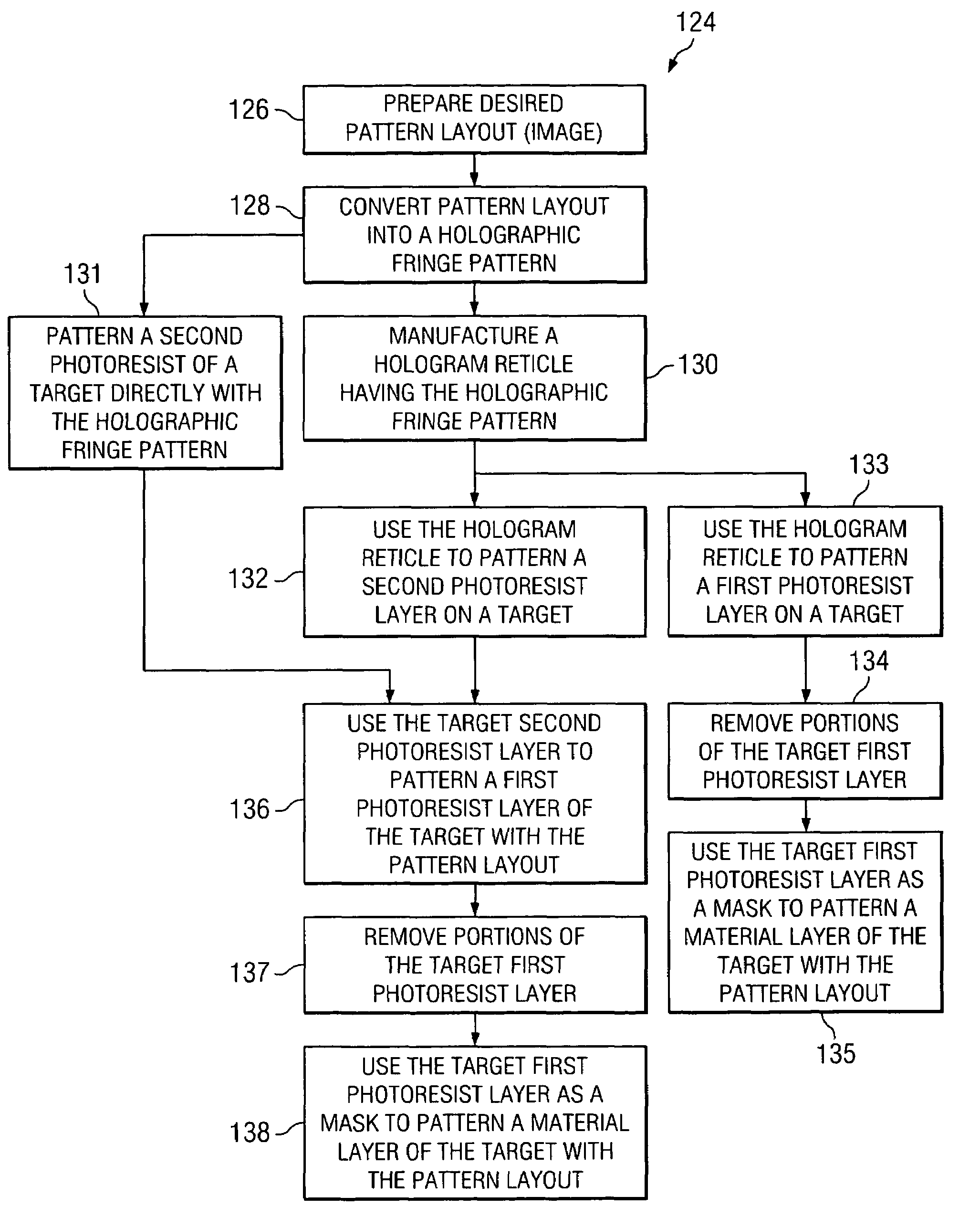
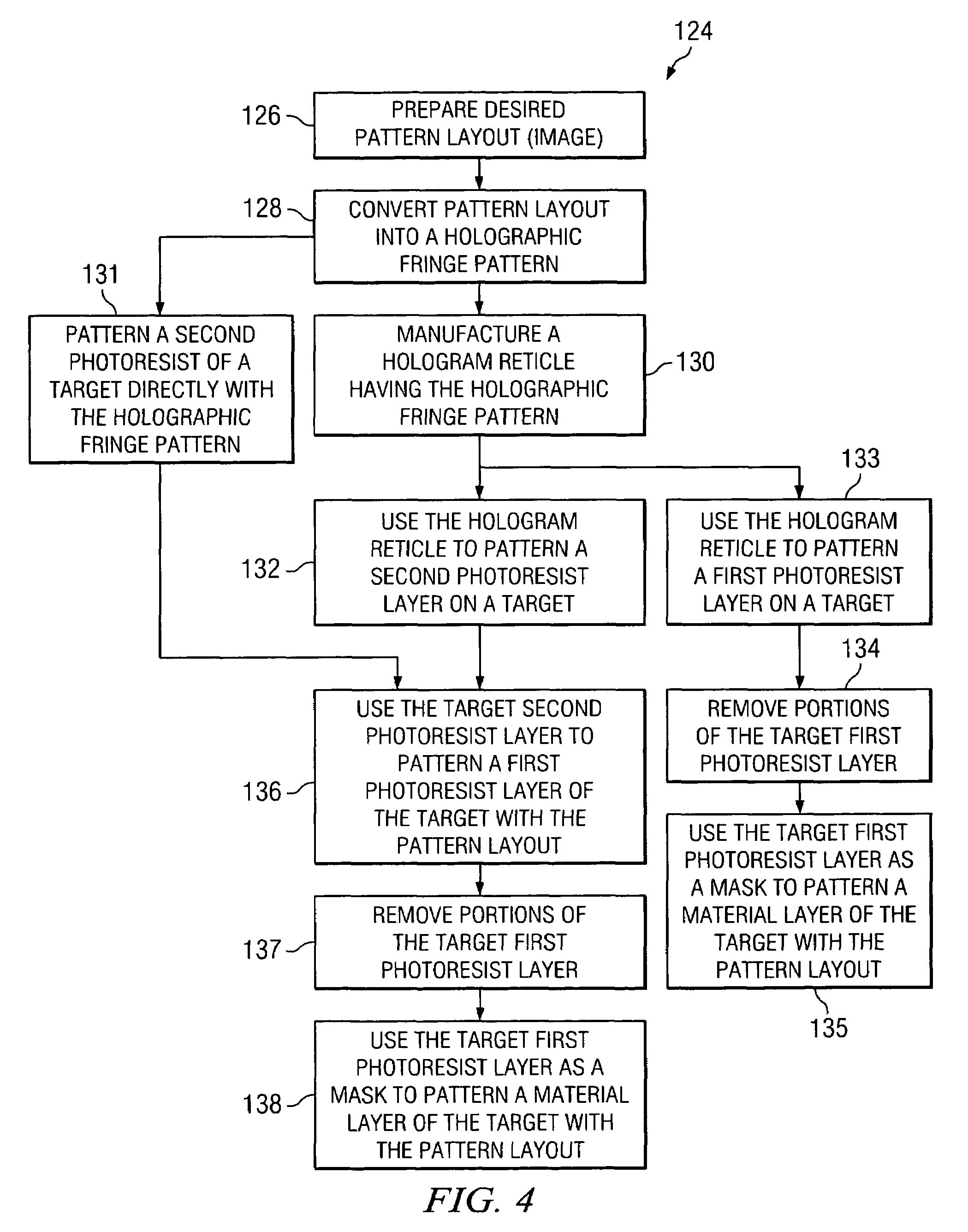
[0052]FIG. 4 is a flow chart 124 illustrating methods of manufacturing and using a hologram reticle in accordance with embodiments of the present invention. First, the desired pattern layout is prepared (step 126). The desired pattern layout, also referred to h...


PUM

PropertyMeasurementUnit
thicknessaaaaaaaaaa
thicknessaaaaaaaaaa
thicknessesaaaaaaaaaa

Abstract

A hologram reticle and method of patterning a target. A layout pattern for an image to be transferred to a target is converted into a holographic representation of the image. A hologram reticle is manufactured that includes the holographic representation. The hologram reticle is then used to pattern the target. Three-dimensional patterns may be formed in a photoresist layer of the target in a single patterning step. These three-dimensional patterns may be filled to form three-dimensional structures. The holographic representation of the image may also be transferred to a top photoresist layer of a top surface imaging (TSI) semiconductor device, either directly or using the hologram reticle. The top photoresist layer may then be used to pattern an underlying photoresist layer with the image. The lower photoresist layer is used to pattern a material layer of the device.

Description

[0001]This application claims the benefit of U.S. Provisional Application No. 60 / 534,721, filed on Jan. 7, 2004, entitled Holographic Reticle and Patterning Method, which application is hereby incorporated herein by reference.REFERENCE TO COMPUTER PROGRAM LISTING APPENDIX[0002]The material on two identical compact disks, Copy 1 and Copy 2, is incorporated herein by reference. Each compact disc contains a file entitled “TSM02-0658, Appendix A”, created on Sep. 18, 2003, having a size of 9 KB.TECHNICAL FIELD[0003]The present invention relates generally to lithography for semiconductor devices, and more particularly to a reticle design including a holographic pattern and methods of patterning a semiconductor wafer using a holographic reticle.BACKGROUND[0004]In semiconductor device manufacturing, features and geometric patterns are created on various layers of semiconductor wafers using optical photolithography. Typically, optical photolithography involves projecting or transmitting ene...

Claims


Application Information

Patent Timeline
Patent Type & Authority Patents(United States)
IPC IPC(8): G03C5/00G03F1/00G03F1/14G03H1/00G03H1/08
CPCG03F1/14G03H1/0005G03H1/0808G03F7/70291G03H2210/452G03H1/0244G03H1/2205G03H2001/0094G03H2001/0833G03H2224/04G03H2240/12G03H2240/13G03H2240/23G03H2270/52G03H2210/30G03F1/50
Inventor CHANG, SHIH-MINGCHANG, CHUNG-HSINGCHIN, CHIH-CHENGWANG, WEN-CHUANLU, CHI-LUNCHIN, SHENG-CHILIN, CHIN-HSIANG
Owner TAIWAN SEMICON MFG CO LTD
Why Eureka
Try Eureka