Fabrication method for a semiconductor structure having integrated capacitors

a technology of integrated capacitors and fabrication methods, which is applied in the direction of capacitors, semiconductor devices, electrical equipment, etc., can solve the problems of reducing the capacitance of the semiconductor structure and reducing the electrical load, and achieves the effect of reducing thermal load, reducing the cost of manufacturing, and increasing the surface area of the capacitor

Inactive Publication Date: 2007-12-25
POLARIS INNOVATIONS LTD
View PDF9 Cites 2 Cited by
  • Summary
  • Abstract
  • Description
  • Claims
  • Application Information

AI Technical Summary

Benefits of technology

[0007]The present invention provides a capacitor concept whose process sequence may be configured in such a way that the capacitor can be created at the very end of the overall process sequence, that is to say e.g. after transistor fabrication or the like. As a result, it is possible to realize substantially lower thermal loading on the capacitor, namely the dielectric layer and the electrodes. Moreover, given the same aspect ratio, substantially larger capacitor surface areas (crown structures) may be made possible, which makes higher capacitance values possible.
[0008]In the case of the method according to the invention, it is possible to keep the rear side of the substrate below a temperature of approximately 400° C. if corresponding deposition processes are chosen. Therefore, ALD (atomic layer deposition) processes, in particular, are taken into consideration. The low process temperature enables an amorphous dielectric layer for the capacitor dielectric with good leakage current properties. An undesirable crystallization of the capacitor layers can be avoided with such process implementation.

Problems solved by technology

In the normal case, trench capacitor concepts also do not permit a crownlike structure of the capacitor, as a result of which electrode area is lost and capacitance is consequently forfeited.

Method used


Image

  • Fabrication method for a semiconductor structure having integrated capacitors
  • Fabrication method for a semiconductor structure having integrated capacitors
  • Fabrication method for a semiconductor structure having integrated capacitors

Examples


first embodiment

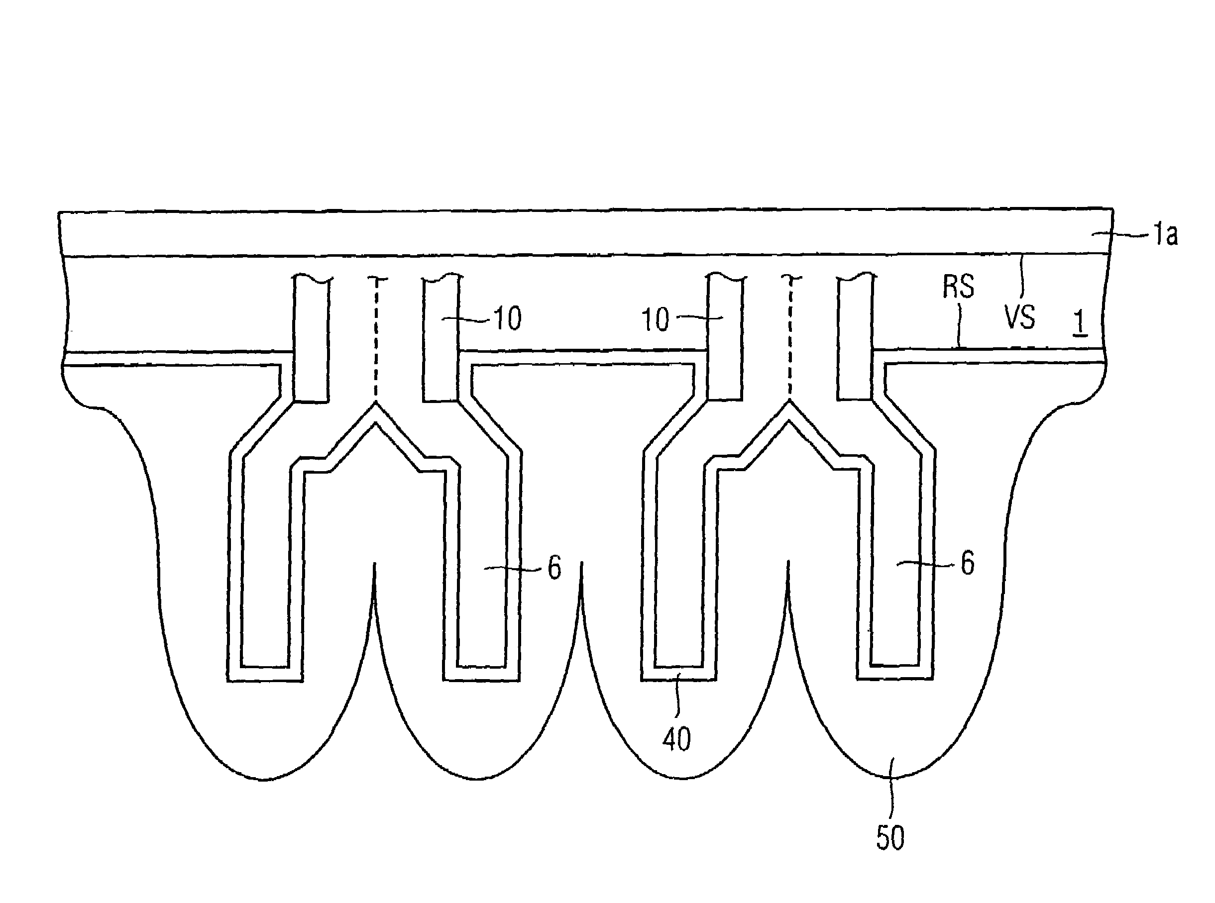
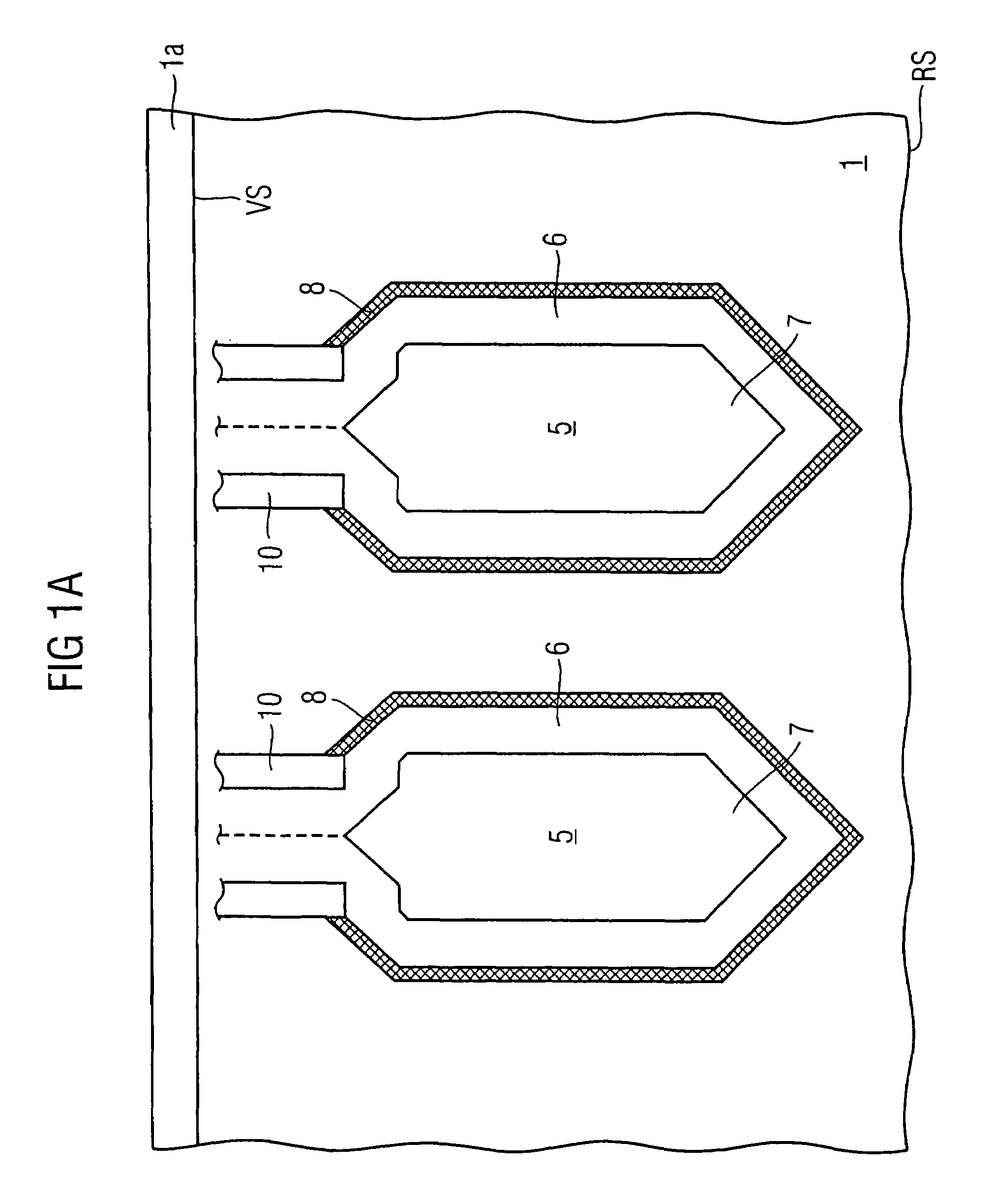
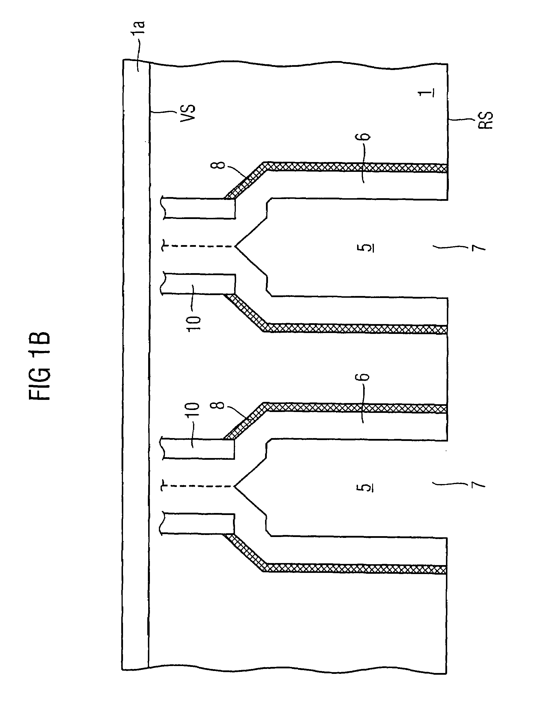
[0050]FIGS. 1A-K show schematic illustrations of successive method stages of a fabrication method for a semiconductor structure as the present invention.

[0051]In FIG. 1A, reference 1 designates a silicon semiconductor substrate having a front side VS and a rear side RS. The front side VS of the semiconductor substrate 1 is connected to a carrier substrate 1A, for example a carrier wafer.

[0052]Trenches 5 are provided in the semiconductor substrate 1, said trenches being widened in bottle-shaped fashion in the lower trench region. The trenches have an insulation collar 10 in the upper trench region. An etching stop layer 8, for example made of Al2O3 or Si3N4, is provided on the trench walls in the interior of the trenches 5. Furthermore, a respective inner capacitor electrode 6, for example made of polysilicon or a metal, is situated in the interior of the trenches 5 on the etching stop layer 8 and leaves a cavity 7 free in the trench.

[0053]For reasons of clarity, that part of the int...

second embodiment

[0065]FIG. 2 shows a schematic illustration of a method stage of a fabrication method for a semiconductor structure as the present invention.

[0066]In the case of the second embodiment shown in FIG. 2, the semiconductor substrate 1 is not removed as far as the level of the insulation collar 10 on the rear side RS, but rather only as far as a region of the trench 5 which lies below the insulation collar 10. The insulation collar 10 made of silicon oxide is protected in this way and is not attacked during later etchings.

[0067]However, in the case of the second embodiment, care must be taken to ensure that the etching stop layer 8 that remains in the shoulder region of the trench has a sufficient thickness in order that a capacitive coupling to the remaining part of the semiconductor substrate 1 can be avoided. In the case of the second embodiment shown in FIG. 2, the semiconductor substrate 1 is not removed as far as the level of the insulation collar 10 on the rear side RS, but rather...

third embodiment

[0068]FIGS. 3A-F show schematic illustrations of successive method stages of a fabrication method for a semiconductor structure as the present invention.

[0069]In accordance with FIG. 3A, the semiconductor substrate comprises a rear-side silicon substrate layer 1′, a front-side silicon substrate layer 1″ and an intervening insulation layer 60, e.g. made of SiO2, which lies at the level of the insulation collars 10. By way of example, a substrate of this type is available as an SOI wafer (silicon-on-insulator).

[0070]Otherwise, the process state shown in FIG. 3A corresponds to the process state in accordance with FIG. 1A.

[0071]Referring further to FIG. 3B, the rear-side silicon substrate layer 1′ is then removed as far as the insulation layer 60 by means of an etching process, the insulation layer 60 serving as an etching stop. In this case, as in the previous embodiments, the inner electrodes are protected by the etching stop layer 8 made e.g. of silicon nitride. The insulation collar...


PUM


Abstract

The present invention provides a fabrication method for a semiconductor structure having integrated capacitors and a corresponding semiconductor structure. The fabrication method has the following steps of: providing a semiconductor substrate (1; 1′, 60, 1″) having a front side (VS) and a rear side (RS); providing trenches (5) in the semiconductor substrate (1; 1′, 60, 1″) proceeding from the front side (VS) of the semiconductor substrate (1; 1′, 60, 1″); providing a respective inner capacitor electrode (6) in the trenches (5); uncovering the inner capacitor electrodes (6) proceeding from the rear side (RS) of the semiconductor substrate (1; 1′, 60, 1″); providing a capacitor dielectric (40) on the uncovered inner capacitor electrodes (6); and providing outer capacitor electrodes (50) on the capacitor dielectric (40) on the inner capacitor electrodes (6).

Description

TECHNICAL FIELD[0001]The present invention relates to a fabrication method for a semiconductor structure having integrated capacitors and a corresponding semiconductor structure.BACKGROUND ART[0002]Although applicable in principle to arbitrary integrated circuits, the present invention and also the problem area on which it is based will be explained with regard to integrated memory circuits using silicon technology.SUMMARY OF THE INVENTION[0003]Nowadays, large scale integrated memory circuits use either trench capacitors or stacked capacitors for storing the bit information.[0004]Trench capacitors expose the capacitor layers to an enormously high thermal budget since the trench is produced before the associated selection transistor and, consequently, the capacitor “sees” the process steps for transistor fabrication. In the normal case, trench capacitor concepts also do not permit a crownlike structure of the capacitor, as a result of which electrode area is lost and capacitance is c...

Claims


Application Information

Patent Timeline
Patent Type & Authority Patents(United States)
IPC IPC(8): H01L21/8242H01L21/02H01L21/334H01L27/08H01L29/94
CPCH01L27/0805H01L29/945H01L28/92H01L29/66181H01L28/91H01L27/1087H10B12/0387
Inventor GUTSCHE, MARTINSEIDL, HARALD
Owner POLARIS INNOVATIONS LTD
Why Eureka
Try Eureka