Cleaning solution for semiconductor substrate

a cleaning solution and semiconductor substrate technology, applied in the direction of detergent compounding agents, inorganic non-surface active detergent compositions, instruments, etc., can solve the problems of difficult removal of ionic foreign substances, particulate foreign substances and ionic foreign substances on the semiconductor substrate after subjecting to cmp, and above cleaning solutions are inferior in wettability with hydrophobic insulating films, etc., to achieve excellent removability

Inactive Publication Date: 2007-12-25
KANTO CHEM CO INC +1
View PDF5 Cites 22 Cited by
  • Summary
  • Abstract
  • Description
  • Claims
  • Application Information

AI Technical Summary

Benefits of technology

[0009]The object of the present invention is to provide a cleaning solution excellent in removability of particulate foreign substances and ionic foreign substances present on a semiconductor substrate after subjected to CMP process.

Problems solved by technology

However, the above cleaning solutions are inferior in wettability with hydrophobic insulating films of low dielectric constant, such as of SiOC, and it is difficult to remove the particulate foreign substances and ionic foreign substances on the semiconductor substrates after subjected to CMP process.

Method used


Image

  • Cleaning solution for semiconductor substrate
  • Cleaning solution for semiconductor substrate
  • Cleaning solution for semiconductor substrate

Examples


example 1

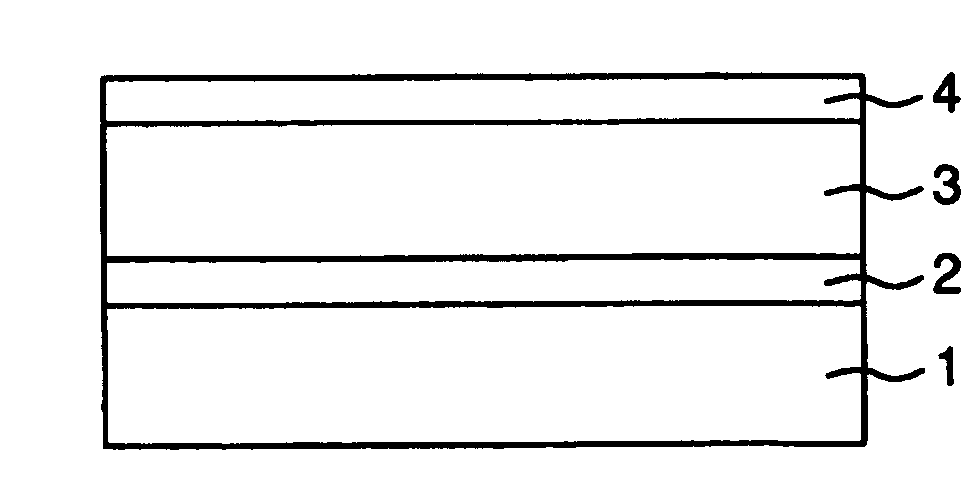
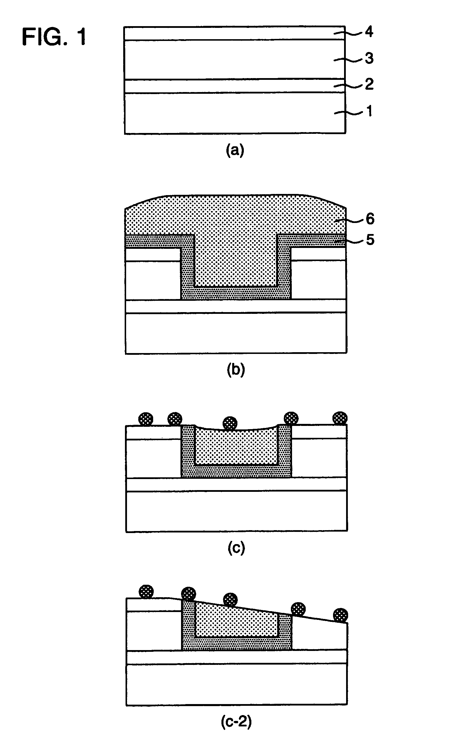
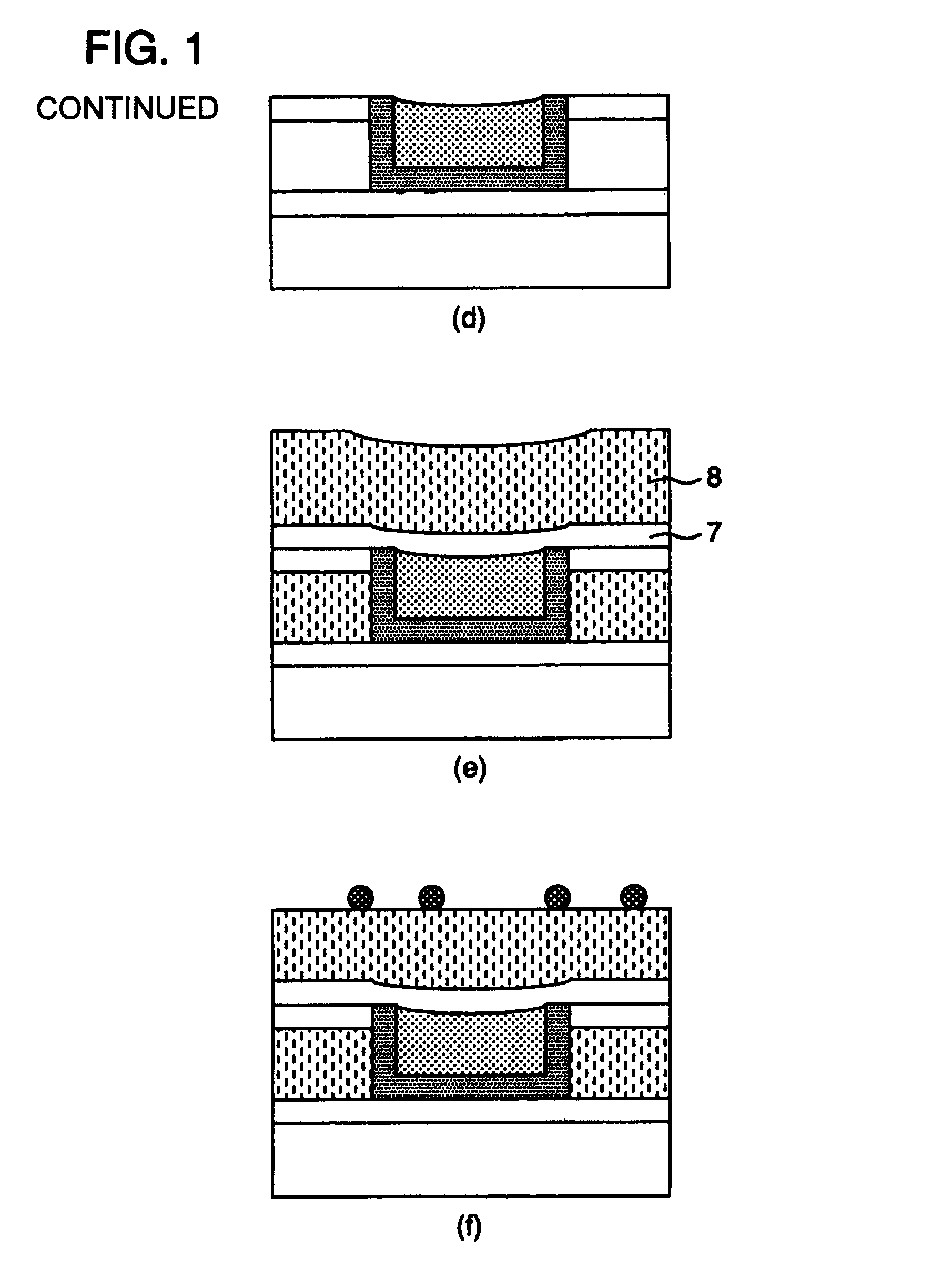
[0076]Cleaning solutions 1 and 2 were prepared following the formulations shown in Table 1. A wafer having an SiOC film which was a kind of an insulating film of low dielectric constant, and the surface of which was previously contaminated with fine particles and metal impurities was cleaned using the cleaning solutions and a brush cleaning apparatus. The concentrations of the remaining fine particles and metal impurities are also shown in Table 1.

[0077]The contamination of the surface of the SiOC film wafer with fine particles before cleaning was conducted by dipping the wafer in a slurry for CuCMP to contaminate the surface of the film with abrasive grains in the slurry. The number of contaminating particles before cleaning was 3000 / wafer. The contamination with metal impurities was conducted by actually polishing the Cu film by CuCMP to contaminate the exposed SiOC film with metals. The degree of contamination with metals before cleaning was 5×10¹² atoms / cm2 in the case of Cu.

[00...


PUM

PropertyMeasurementUnit
relative dielectric constantaaaaaaaaaa
semiconductoraaaaaaaaaa
oleophilicaaaaaaaaaa

Abstract

A cleaning solution for semiconductor substrates comprising a nonionic surface active agent of the formula (1) and/or the formula (2), a chelating agent and a chelating accelerator:
CH3—(CH2)l—O—(CmH2mO)n—X   (1)
wherein l, m and n independently represent a positive number, and X represents a hydrogen atom or a hydrocarbon group;
CH3—(CH2)a—O—(CbH2bO)d—(CxH2xO)y—X   (2)
wherein a, b, d, x and y independently represent a positive number, b and x are different, and X represents a hydrogen atom or a hydrocarbon group.

Description

BACKGROUND OF THE INVENTION[0001]1. Field of the Invention[0002]The present invention relates to a cleaning solution for semiconductor substrates.[0003]2. Description of Related Art[0004]Recently, Cu wiring is introduced into semiconductor devices, and for the formation of Cu wiring, a chemical and mechanical polishing process (CMP process) is employed.[0005]This CMP process comprises forming grooves or connecting holes in a previously flattened insulating film of low dielectric constant, such as of carbon-containing SiO2 (SiOC), then forming a Cu film, for example by plating method to fill the grooves or connecting holes, and polishing the surface with a slurry containing special abrasive grains and additives to remove Cu in the portions other than the grooves or connecting holes, thereby flattening the surface and forming the wiring or connecting holes.[0006]On the semiconductor substrate after subjected to the CMP process, there are fine foreign particulate substances such as abr...

Claims


Application Information

Patent Timeline
Patent Type & Authority Patents(United States)
IPC IPC(8): C11D1/72C11D1/722C11D7/08C11D9/22C11D3/20C11D3/33C11D3/36C11D11/00H01L21/02H01L21/306H01L21/3105H01L21/321
CPCC11D1/722C11D3/2086C11D3/2093H01L21/02074C11D3/361C11D11/0047H01L21/02065C11D3/33C11D1/72
Inventor TAKASHIMA, MASAYUKIKASAMA, YOSHIKOTOMIMORI, HIROAKIAOKI, HIDEMITSU
Owner KANTO CHEM CO INC
Why Eureka
Try Eureka