Cleaning composition, method for producing semiconductor device, and cleaning method

a cleaning composition and semiconductor technology, applied in detergent compositions, detergent mixture preparations, chemistry apparatus and processes, etc., can solve the problems of tungsten corroding during cleaning in some cases, and achieve the effect of excellent removal of plasma etching residues

Active Publication Date: 2011-11-17
FUJIFILM CORP
View PDF4 Cites 24 Cited by
  • Summary
  • Abstract
  • Description
  • Claims
  • Application Information

AI Technical Summary

Benefits of technology

[0009]However, it is known that tungsten exposed by misalignment is deformed into a state which is susceptible to corrosion after the ashing step, and with conventional cleaning liquids, tungsten may corrode during cleaning in some cases. Thus, there has been a demand for a cleaning composition which can maintain the cleaning performance and inhibit the corrosion of tungsten. Further, it has been required to inhibit the corrosion of other metals such as aluminum, copper, and the like, in addition to the cleaning performance and the inhibition of the corrosion of tungsten.
[0010]Thus, the present invention has been made in consideration of the above-problems, and it is an object of the present invention to provide a cleaning composition, which can inhibit the corrosion of metals such as tungsten, aluminum, and the like of the semiconductor substrate, and has an excellent removability of plasma etching residues and / or ashing residues on the semiconductor substrate, a method for producing a semiconductor device, and a cleaning method using the cleaning composition.
[0024]Due to the present invention, the corrosion of a metal of the semiconductor substrate can be inhibited, and a cleaning composition having an excellent removability of plasma etching residues and / or ashing residues on the semiconductor substrate, a method for producing a semiconductor device, and a cleaning method using the cleaning composition can be provided.

Problems solved by technology

However, it is known that tungsten exposed by misalignment is deformed into a state which is susceptible to corrosion after the ashing step, and with conventional cleaning liquids, tungsten may corrode during cleaning in some cases.

Method used


Image

  • Cleaning composition, method for producing semiconductor device, and cleaning method
  • Cleaning composition, method for producing semiconductor device, and cleaning method
  • Cleaning composition, method for producing semiconductor device, and cleaning method

Examples


first embodiment

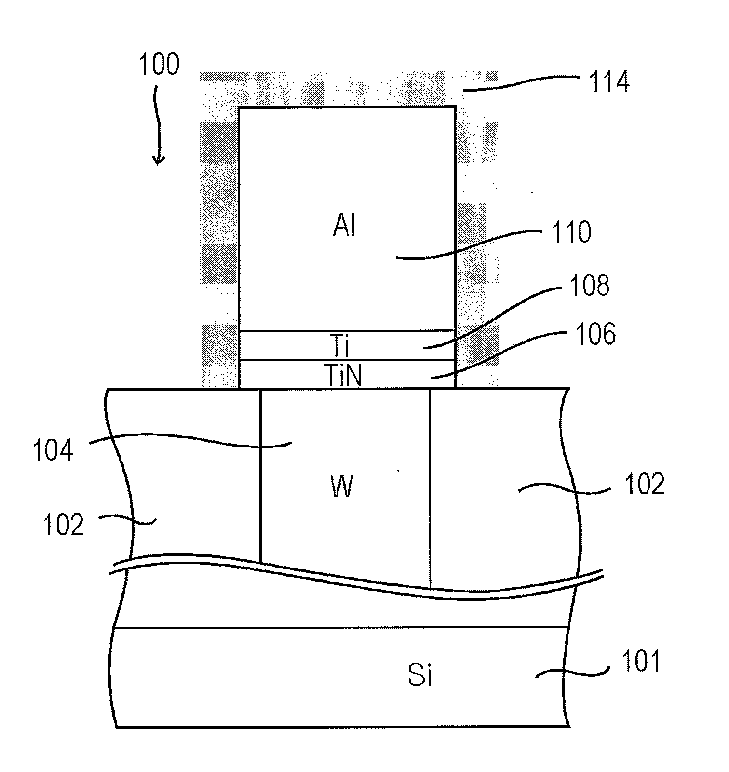
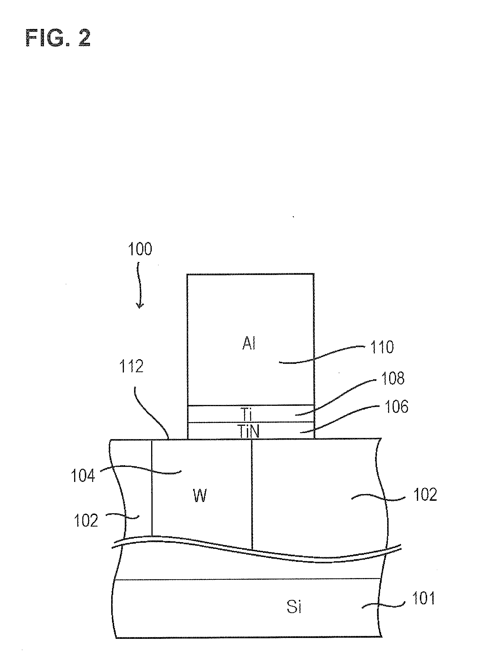
[0134]The outline of a method for producing a semiconductor device according to the first embodiment of the present invention is described with reference to FIGS. 1 to 3.

[0135]FIG. 1 is a schematic cross-sectional view showing the wiring pattern at an ordinary time in one embodiment of the method for producing a semiconductor device of the present invention, and FIG. 2 is a schematic cross-sectional view showing the wiring pattern at misalignment in one embodiment of the method for producing a semiconductor device of the present invention.

[0136]Furthermore, FIG. 3 is a schematic cross-sectional view of the semiconductor device showing a state in which the plasma etching residues and / or the ashing residues are adhered after ashing.

[0137]FIG. 1 shows a substrate 100, in which a wiring pattern (a structure formed of an Al alloy film 110, a titanium film 108, and a titanium nitride film 106) is provided on a tungsten plug 104 formed between the interlayer insulating films 102 on a semic...

second embodiment

[0148]FIG. 4 is a step cross-sectional view showing the outline in another embodiment (the second and third embodiments) of the method for producing a semiconductor device of the present invention.

[0149]First, an element other than a transistor or one layer or two or more layers of a wiring is formed on the semiconductor substrate 10 such as a silicon wafer and the like by an ordinary process for producing a semiconductor device. Then, an interlayer insulating film is formed on the semiconductor substrate 10 on which an element or the like has been formed.

[0150]Then, an Al alloy film 12 for example, having a film thickness of about 500 nm and a titanium nitride film 14, for example, having a film thickness of about 50 nm are sequentially laminated on the front face, for example, by a CVD (Chemical Vapor Deposition) method. Thus, a conductor film including the Al alloy film 12 and the titanium nitride film 14 sequentially laminated thereon is formed. Further, the Al alloy film 12 is ...

third embodiment

[0160]Next, the outline of method for producing a semiconductor device according to the third embodiment of the present invention is similarly described with reference to FIG. 4.

[0161]The method for producing a semiconductor device according to the third embodiment of the present invention is different from the method for producing a semiconductor device according to the second embodiment, in that a via hole 22 reaching the Al alloy film 12 of the wiring 16 is formed.

[0162]First, in the same manner as the method for producing a semiconductor device according to the second embodiment, the wiring 16 including the Al alloy film 12 and the titanium nitride film 14, and the silicon oxide film 18 are formed on the semiconductor substrate 10 (see FIG. 4(a)).

[0163]Then, a photoresist film having a via pattern is formed on the silicon oxide film 18 by photolithography. Subsequently, the silicon oxide film 18 and the titanium nitride film 14 are etched by dry etching using a plasma with this ...


PUM

PropertyMeasurementUnit
pHaaaaaaaaaa
thicknessaaaaaaaaaa
thicknessaaaaaaaaaa

Abstract

Provided are a cleaning composition which is capable of inhibiting the metal of a semiconductor substrate from corrosion, and has an excellent removability of plasma etching residues and / or ashing residues on the semiconductor substrate, a method for producing a semiconductor device, and a cleaning method using the cleaning composition. The cleaning composition for removing plasma etching residues and / or ashing residues formed on a semiconductor substrate, and a preparation method and a cleaning method for a semiconductor device, using the cleaning composition, wherein the cleaning composition includes (Component a) water; (Component b) an amine compound; (Component c) hydroxylamine and / or a salt thereof; (Component d) a quaternary ammonium compound; (Component e) an organic acid; and (Component f) a water-soluble organic solvent; and has a pH of 6 to 9.

Description

BACKGROUND OF THE INVENTION[0001]1. Field of the Invention[0002]The present invention relates to a cleaning composition, a method for producing a semiconductor device, and a cleaning method.[0003]2. Description of the Related Art[0004]In the production of semiconductor integrated circuits, progress is being made in terms of increases in scale, increases in density, and miniaturization. In the production of integrated circuits, a lithography step in which a positive type or negative type photoresist is used is employed. A resist film provided on a semiconductor substrate by coating is exposed by an exposure plate such as a photomask or the like. The pattern formed by a photochemical change in the resist film becomes a resist pattern having a shape corresponding to the exposure plate by development. In order to improve the etching resistance of the resist pattern, a post-bake or UV curing is carried out, as needed. The obtained resist pattern is used as a mask to carry out etching or ...

Claims


Application Information

Patent Timeline
Patent Type & Authority Applications(United States)
IPC IPC(8): H01L21/3065C11D7/60
CPCC11D7/265C11D7/3209C11D11/0047C11D7/5004C11D7/3218
Inventor INABA, TADASHITAKAHASHI, KAZUTAKATAKAHASHI, TOMONORIMIZUTANI, ATSUSHI
Owner FUJIFILM CORP
Why Eureka
Try Eureka