Nonvolatile semiconductor memory apparatus

a semiconductor memory and apparatus technology, applied in semiconductor devices, digital storage, instruments, etc., can solve the problems of increasing manufacturing costs, increasing the number of advanced masks and processing steps, and inherently complex flash memory, so as to reduce overall costs, reduce manufacturing costs, and save silicon wafers. cost

Inactive Publication Date: 2008-01-08
ATMEL CORP
View PDF13 Cites 36 Cited by
  • Summary
  • Abstract
  • Description
  • Claims
  • Application Information

AI Technical Summary

Benefits of technology

[0007]A nonvolatile memory apparatus where high level functions of “storage,”“retrieval,” and “control” are separated and implemented in two or more separate semiconductor subsystems (for example, fabricating memory storage functions independently from memory control functions). A simple device, memory for example, could be fabricated in one layer and more complex devices (e.g., control and high voltage circuits) could be fabricated in another layer. Therefore, ubiquitous monolithic nonvolatile memory device of contemporary manufacture is implemented in a more cost efficient way with overall higher manufacturing yield. The higher efficiency does not come, however, at the detriment of memory performance, as each subsystem of the present invention is fabricated with a process most suitable for a specific circuit.
[0009]For an integrated circuit chip incorporated control function (e.g., an integrator / companion-control interface circuit), a relatively more expensive process is employed without requiring the complex lithographic, steps, and masks to be used on the memory circuit. Since the integrator / companion-control interface circuit area is much smaller than that of the memory circuit, an important cost saving per silicon wafer is achieved as many more integrator / companion-control interface circuits may be produced per wafer and enhanced yield is achieved.
[0010]In an exemplary embodiment, the nonvolatile memory apparatus thus includes a separate integrator / companion-control interface circuit and memory circuit. The integrator / companion-control interface circuit is fabricated on a first integrated circuit chip. The integrator / companion-control interface circuit includes a plurality of charge pump circuits, a system interface logic circuit, a memory control logic circuit, and one or more analog circuits. The memory circuit is fabricated on a second integrated circuit chip and includes a column decoder, a row decoder, a control register, and a data register. A memory-companion-control interface area includes a first plurality of die bond pads on the first integrated circuit chip and a second plurality of die bond pads on the second integrated circuit chip such that the two chip components may be die-bonded together. Additionally, a single integrator / companion-control interface circuit may interface with a plurality of memory circuits, thus further reducing overall costs on a per-memory basis, as each memory circuit does not require a dedicated integrator / companion-control interface circuit.

Problems solved by technology

As density and read / program bandwidth requirements continue to increase, flash memories are becoming inherently more complex, both from a design and manufacturing standpoint.
Hence, as the lithography advances to produce smaller and consequently more cost effective devices, such integration requires a commensurate increase in the number of advanced masks and processing steps.
This increased complexity results in increased manufacturing costs and limits an economic scalability of future memory devices.

Method used


Image

  • Nonvolatile semiconductor memory apparatus
  • Nonvolatile semiconductor memory apparatus
  • Nonvolatile semiconductor memory apparatus

Examples


Embodiment Construction

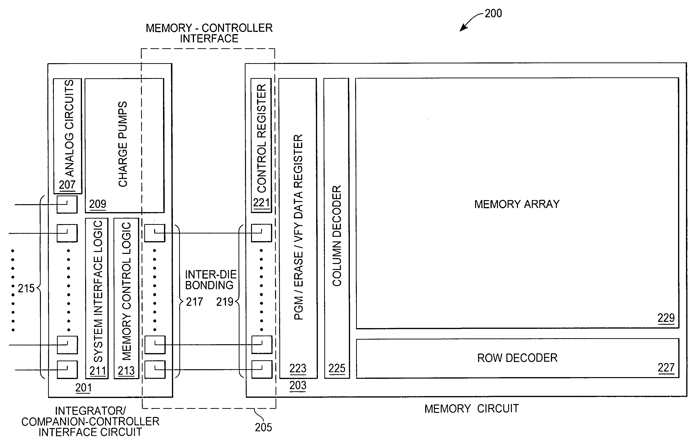
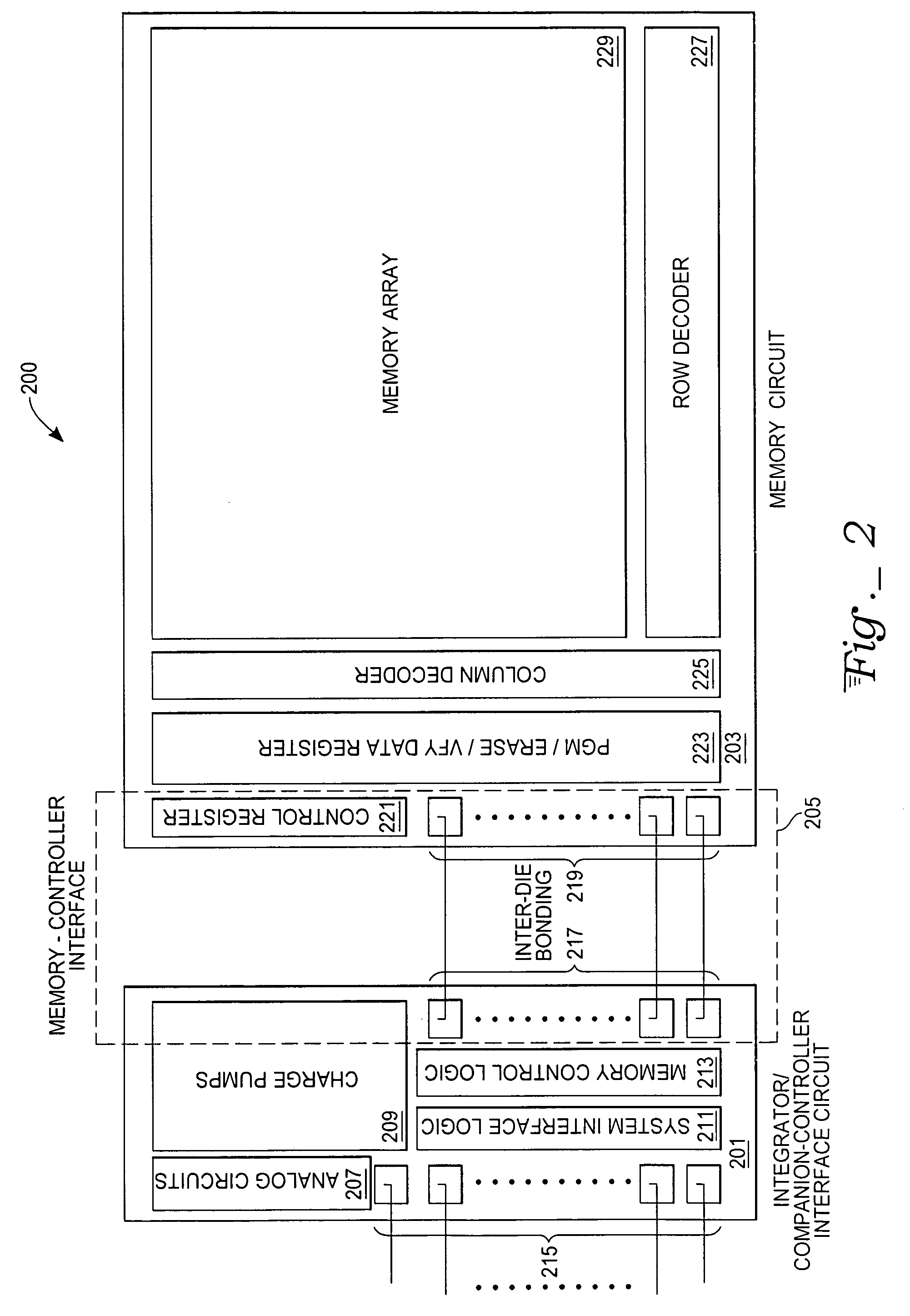
[0016]With reference to FIG. 2, an exemplary nonvolatile memory apparatus 200 includes an integrator / companion-control interface circuit 201, a memory circuit 203, and a memory-companion-control interface 205. Components of the integrator / companion-control interface circuit 201 include a plurality of analog circuits 207, a plurality of charge pumps 209, a system interface logic circuit 211, a memory interface logic circuit 213 and datapath logic to provide fast access for data passing to and from the memory circuit 203. The integrator / companion-control interface circuit 201 also includes a plurality of host system-controller interface pads 215, allowing bidirectional communications with one or more external host systems (not shown), and a plurality of integrator / companion-control interface circuit inter-die bonding pads 217, allowing bidirectional communications between the integrator / companion-control interface circuit 201 and the memory circuit 203 through a plurality of memory ci...


PUM


Abstract

A nonvolatile memory apparatus includes a separate controller circuit and memory circuit. The controller circuit is fabricated on a first integrated circuit chip. The controller circuit includes a plurality of charge pump circuits, a system interface logic circuit, a memory control logic circuit, and one or more analog circuits. The memory circuit is fabricated on a second integrated circuit chip and includes a column decoder, a row decoder, a control register, and a data register. A memory-controller interface area includes a first plurality of die bond pads on the first integrated circuit chip and a second plurality of die bond pads on the second integrated circuit chip such that the first and second integrated circuit chips may be die-bonded together. A single controller circuit may interface with a plurality of memory circuits, thus further reducing overall costs as each memory circuit does not require a dedicated controller circuit.

Description

TECHNICAL FIELD[0001]The present invention relates to nonvolatile memory circuits. More specifically, the invention relates to multi-component memory integrated circuits.BACKGROUND ART[0002]An increasing demand for portable digital storage media for equipment such as digital cameras, handheld gaming consoles, and audio players has created a need for high-density nonvolatile memories. For such applications, flash memory technology has been successfully developed and employed.[0003]As density and read / program bandwidth requirements continue to increase, flash memories are becoming inherently more complex, both from a design and manufacturing standpoint. A basic requirement for a flash process is a set of high voltage rules and associated masks that define the memory cell array, surrounded by its row and column decoding circuits. Triple well processes are commonly used and gate oxide thicknesses ranging from 180 Å to 300 Å are typically required for the flash cell and high voltage sele...

Claims


Application Information

Patent Timeline
Patent Type & Authority Patents(United States)
IPC IPC(8): G11C5/06
CPCG11C7/10H01L2224/05553H01L2224/48137H01L2224/49175
Inventor TELECCO, NICOLAADUSUMILLI, VIJAY P.GUPTA, ANILHUI, EDWARDSCHUMANN, STEVEN J.
Owner ATMEL CORP
Why Eureka
Try Eureka