Unlock instant, AI-driven research and patent intelligence for your innovation.

Semiconductor device inspection method

a semiconductor and device technology, applied in the direction of individual semiconductor device testing, semiconductor/solid-state device testing/measurement, instruments, etc., can solve the problems of large amount of time required in all inspection operations, complex operation, and large number of inspection conditions. , to achieve the effect of reducing user inpu

Inactive Publication Date: 2008-02-19
HITACHI LTD
View PDF12 Cites 21 Cited by
  • Summary
  • Abstract
  • Description
  • Claims
  • Application Information

AI Technical Summary

Benefits of technology

[0012]The present invention provides a technology for inspecting intricate circuit patterns that uses images formed by irradiating white light, laser light, or an electron beam, and that minimizes user input by using semiconductor device design data when setting the various conditions required for inspection.
[0013]By using semiconductor device design data, the present invention also provides a technology that temporarily determines the above inspection condition settings before semiconductor devices requiring inspection reach the inspection process. This minimizes the time taken to set inspection conditions.
[0014]By using semiconductor device design data, the present invention further provides a technology that produces inspection results, the number of false alarms caused by the highly sensitive inspection that occur during defect detection being held below a certain percentage thereof.
[0016]By using semiconductor device design data, the present invention further provides a technology that enables inspection sensitivity to be set to any level to suit the design rules for each area within a semiconductor device chip or to suit the degree of functional importance.
[0020]The present invention is also equipped with a function that, through the use of semiconductor device design data, increases the number of detection signal parameters from specific repetitive patterns used in statistical processing during defect detection.
[0021]According to the present invention, a semiconductor device inspection device is further equipped with a function that, through the use of semiconductor device design data, adds, to detection results, information as to whether or not the area in which a defect was detected is one in which false alarms tend to occur. The present invention is also equipped with a function that, based on this supplementary information, can isolate and review those defects in areas in which false alarms tend to occur.

Problems solved by technology

However, there are no descriptions of the procedures or operation methods for these inspection condition settings for the above conventional devices and their operation is complex, between one and several hours being required to set appropriate inspection conditions for a new wafer to be inspected.
A problem exists in that, in order to implement pattern inspections for a plurality of products (that is a plurality of circuit pattern matrices) and a plurality of processes (that is a plurality of materials and a plurality of detailed circuit pattern forms) in a semiconductor manufacturing line, a huge number of inspection conditions must be set.
As a result, an enormous amount of time is required in all inspection operations and in particular, in inspection condition setting operations.
Furthermore, while conditions are being extracted, there is an accumulation of semiconductor products.
Therefore, the turnaround time (TAT) of semiconductor devices is extended and costs increase.

Method used


Image

  • Semiconductor device inspection method
  • Semiconductor device inspection method
  • Semiconductor device inspection method

Examples


Embodiment Construction

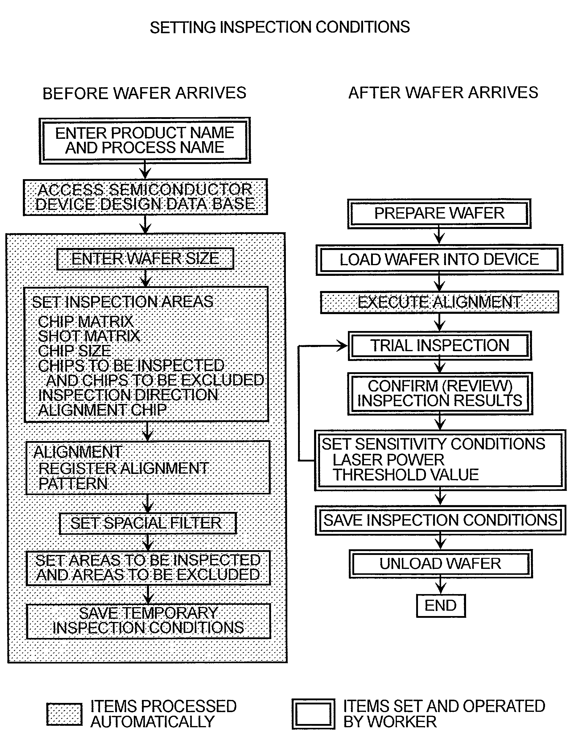
[0048]FIG. 2 shows an example of a sequence relating to the setting of inspection conditions according to the present invention. Firstly, inspection conditions are temporarily determined prior to the wafer actually arriving at the inspection process. This enables minimization of wafer accumulation time while conditions are being set.

[0049]Firstly, the product name of the semiconductor device to be inspected and the name of the process in which the semiconductor device is processed immediately prior to inspection are entered from a terminal. When the product name and process name are entered, the semiconductor device design data base is accessed via a communication means and the data required for inspection preliminary preparation collected. The conditions required for inspection are then automatically set in the steps sown in FIG. 2. A worker can enter the product name and process name settings by any means such as a keyboard or a barcode reader. Entries can be made from within a cl...


PUM


Abstract

Techniques for inspecting semiconductor devices. An inspection condition using chip matrix data and chip size data is set. The intricate circuit patterns of at least one semiconductor device is inspected with the inspection condition. In an embodiment of the present invention, inspection uses images formed by the irradiation of white light, a laser light, or an electron beam. Data obtained from the inspection is used to generate a revised inspection condition. Semiconductor devices are inspected using the revised inspection condition.

Description

BACKGROUND OF THE INVENTION[0001]1. Field of the Invention[0002]The present invention relates to a method for inspecting semiconductor devices, liquid crystals, and magnetic heads.[0003]An example in which a semiconductor wafer is inspected will be explained.[0004]2. Description of the Related Art[0005]Semiconductor devices are manufactured by repeating a process that uses lithography or etching to transfer a pattern, usually formed on a photomask, onto a semiconductor wafer. In a semiconductor device manufacturing process, the quality of the lithography or etching, the quality of various other types of processing, and the production of foreign matter can greatly affect the semiconductor device yield. Therefore, methods for inspecting semiconductor wafers from a manufacturing process have conventionally been implemented to detect anomalies or faults early or before they occur.[0006]Methods for inspecting for defects in patterns on semiconductor wafers involve the use of a defect ins...

Claims


Application Information

Patent Timeline
IPC IPC(8): H01L21/66G01N23/225G01N21/95G01N21/956G06T1/00H01L21/00
CPCG01N21/9501G01N21/95607H01L21/67271G01N2021/95615
Inventor HAMAMATSU, AKIRANOGUCHI, MINORIOHSHIMA, YOSHIMASANISHIYAMA, HIDETOSHI
Owner HITACHI LTD
Features
  • R&D
  • Intellectual Property
  • Life Sciences
  • Materials
  • Tech Scout
  • Unparalleled Data Quality
  • Higher Quality Content
  • 60% Fewer Hallucinations
Learn More