Optical receiver

a receiver and optical technology, applied in the field of optical receivers, can solve the problems of constant change, signal pulse string timing differences on transmission, and signal-to-noise ratio (sn ratio) during data identification to degrade,

Inactive Publication Date: 2008-02-19
OKI ELECTRIC IND CO LTD
View PDF11 Cites 2 Cited by
  • Summary
  • Abstract
  • Description
  • Claims
  • Application Information

AI Technical Summary

Problems solved by technology

The cross-correlation waveform becomes noise with respect to the desired signal, thereby causing the signal-to-noise ratio (SN ratio) during data identification to degrade.
However, the timing of the desired signal must be extracted from a coded multiplexed signal in which the noise level is changing.
Furthermore, the signal is transmitted through optical fiber that is affected by temperature fluctuations and other environmental factors, so the timing of the signal pulse string differs on the transmission and receiving sides, and is constantly changing with time.
However, a large number of optical elements are required to realize a time gate, and the system is made more expensive as a result.
Also, the polarization state of the optical clock and the decoded optical signal are fixed in a desired shape, so adjustments must be made with a polarization state control device in addition to many aspects that require adjustment, and adjustment work is complicated.

Method used


Image

  • Optical receiver
  • Optical receiver
  • Optical receiver

Examples


first embodiment

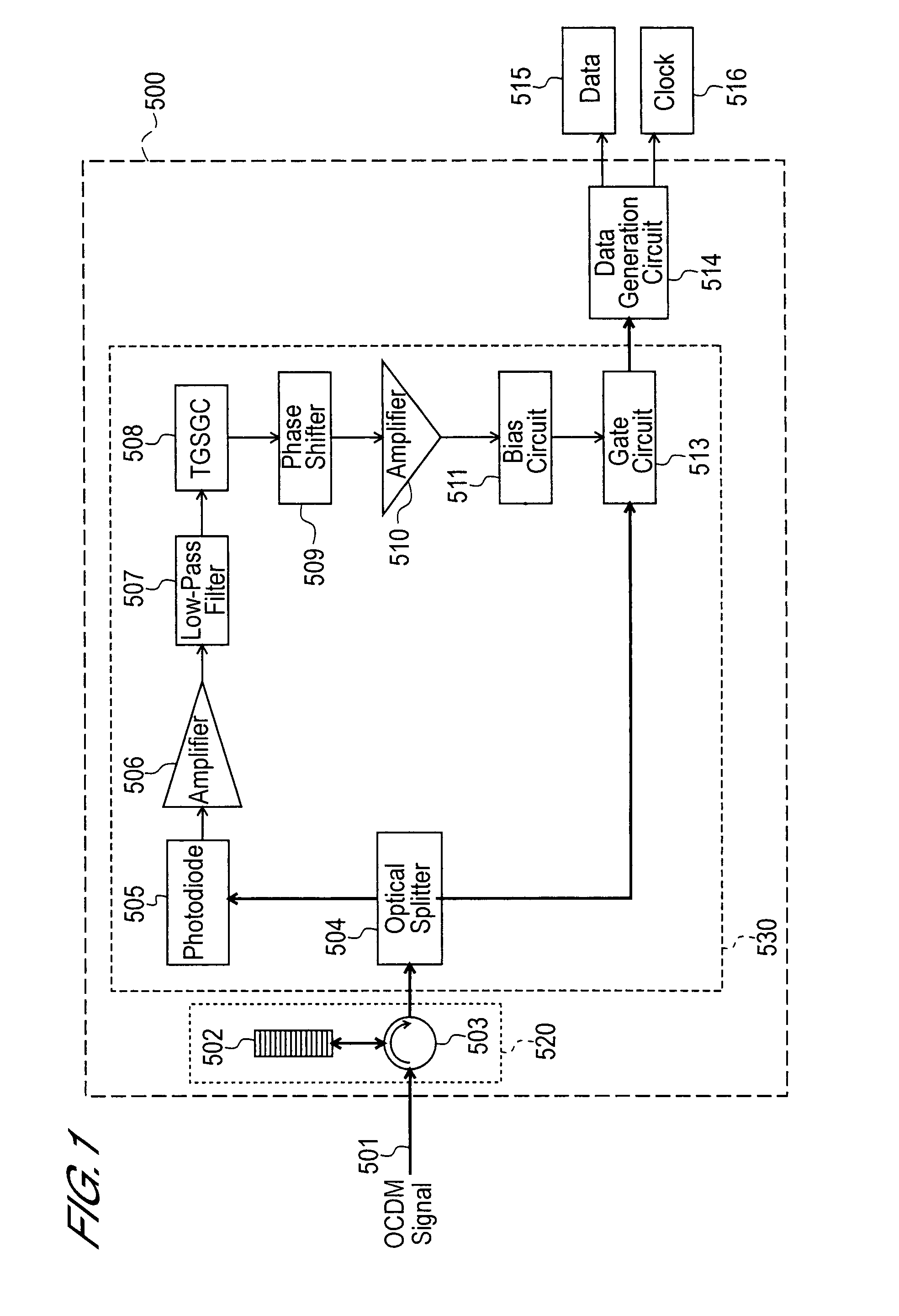
[0032]The first embodiment of the optical receiver of the present invention is described in detail below with reference to the drawings. In the drawings, optical signal paths are indicated by thick lines, and electrical signal paths are indicated by thin lines. Numbers assigned to these thick and thin lines, in addition to denoting the paths themselves, also denote the optical signals or electrical signals which are propagated in the respective paths.

[0033]FIG. 1 is a block diagram showing the entire configuration of the optical receiver 500 of the first embodiment.

[0034]The optical receiver 500 of the first embodiment comprises a decoding circuit 520, a time gate circuit 530, and a data regeneration circuit 514.

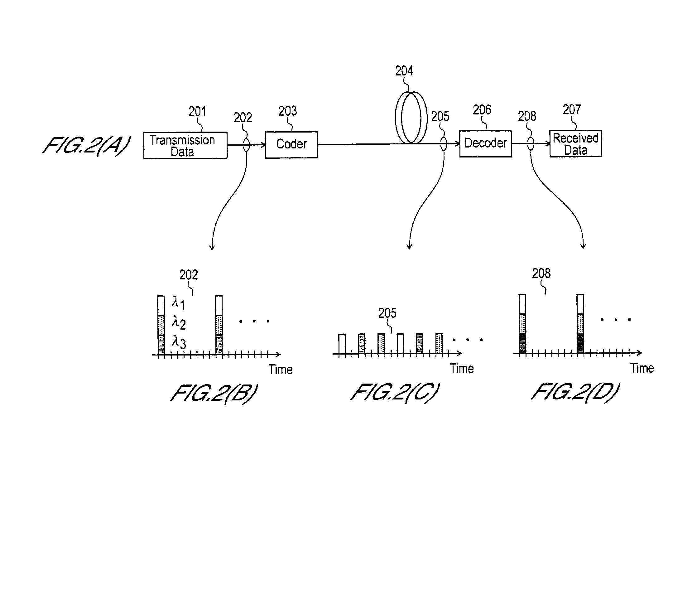
[0035]The decoding circuit 520 comprises a circulator 503 and a fiber Bragg grating (FBG) 502. The decoding circuit 520 is provided as a decoding circuit for an OCDM signal 501 (refer to FIG. 4(D)) transmitted by way of a transmission line (optical fiber, for example).

[0036]...

second embodiment

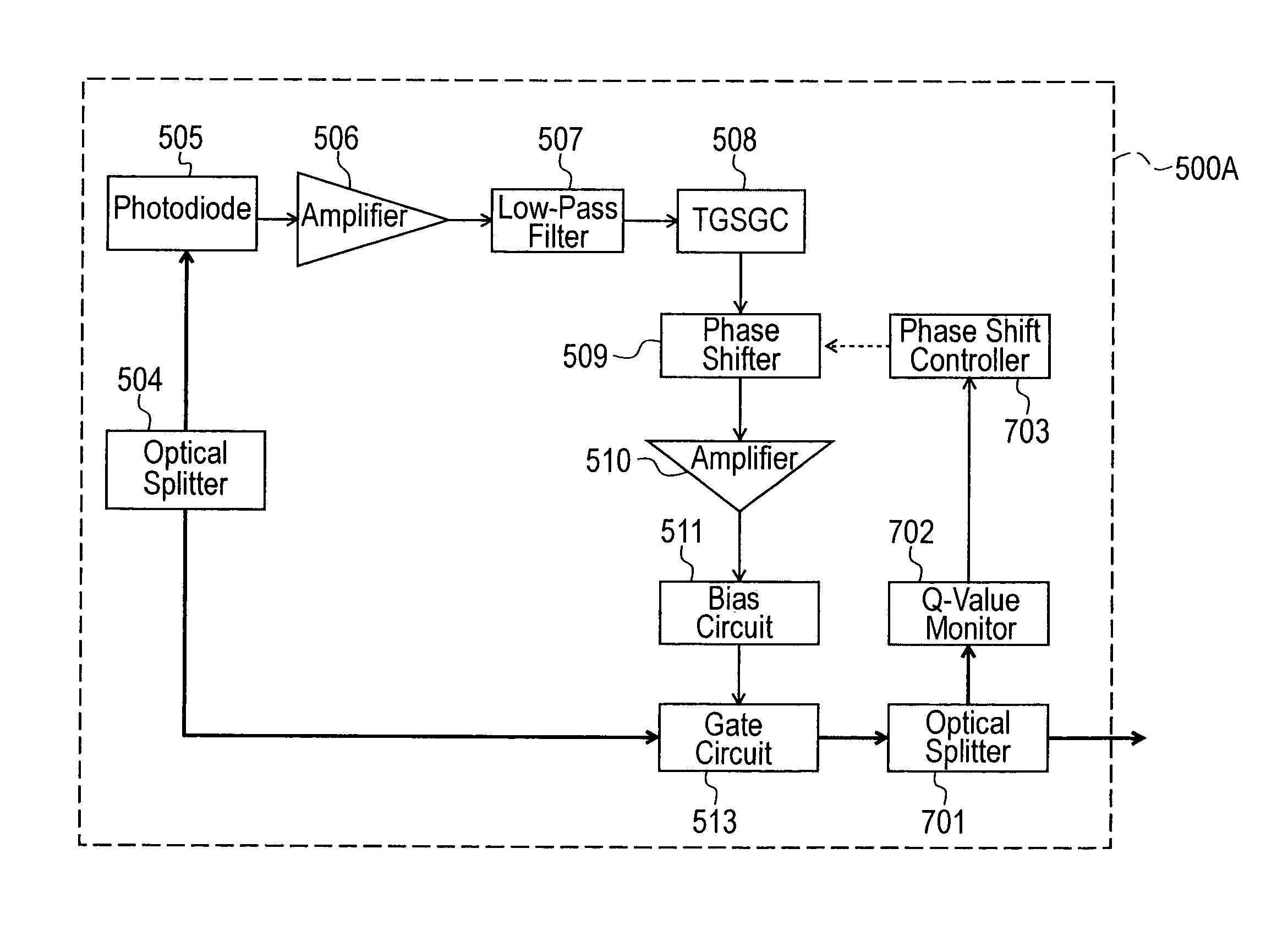
[0054]Next, the second embodiment of the optical receiver of the present invention is described in detail with reference to the diagrams.

[0055]FIG. 8 is a block diagram showing a detailed configuration of a time gate circuit in the optical receiver 500A of the second embodiment, and a depiction of the decoding circuit and the data regeneration circuit is omitted. In FIG. 8, the same symbols are assigned to portions (constituent elements) that correspond to FIG. 1, which describes the first embodiment.

[0056]In addition to the configuration of the first embodiment, the time gate circuit of the second embodiment comprises an optical splitter 701, a Q-value monitor 702, and a phase shift controller 703, as is apparent from the a comparison of FIGS. 1 and 8.

[0057]The optical splitter 701 splits the optical signal outputted by the gate circuit 513 into two, one split optical signal is fed to the data regeneration circuit, which is not depicted (refer to FIG. 1), and the other split optica...

third embodiment

[0065]Next, the third embodiment of the optical receiver of the present invention is briefly described with reference to the diagrams.

[0066]FIG. 9 is a block diagram showing a detailed configuration of a time gate circuit in the optical receiver 500B of the third embodiment, and a depiction of the decoding circuit and the data regeneration circuit is omitted. In FIG. 9, the same symbols are assigned to portions (constituent elements) that correspond to FIG. 8, which describes the second embodiment.

[0067]In the time gate circuit in the optical receiver 500B of the third embodiment, the phase shifter 509 is omitted and an optical delay device 801 for varying the delay time by means of a control signal from a delay controller 703A is disposed instead in the optical path of the optical splitter 504 and photodiode 505.

[0068]In other words, the optical receiver 500B of the third embodiment is configured so that the timing of the time gate signal fed to the gate circuit 513 can be adjusted...


PUM


Abstract

There is provided an optical receiver in which a time gate can be realized with a simple, low-cost configuration, and which has few aspects that require adjustment. The optical receiver of the present invention comprises a decoding circuit in which optical signals which are spread over time in accordance with a coding pattern are inputted and decoded in accordance with a decoding pattern; and a time gate circuit for generating a time gate signal that represents the interval of time in which a significant optical pulse is present in the decoded optical signal, and controlling the passage of the decoded optical signal. The time gate circuit comprises optical splitting means for splitting the decoded optical signal from the decoding circuit into two, optical/electric conversion means for converting one of the split optical signals into an electric signal, time gate signal generation means for generating a time gate signal whose frequency is the fundamental frequency component in synchronism with the electric signal, and gate means for controlling the passage of the other split decoded optical signal in accordance with the time gate signal.

Description

BACKGROUND OF THE INVENTION[0001]1. Field of the Invention[0002]The present invention relates to an optical receiver, and more particularly to an optical receiver that can be applied to waveform shaping for decoded light in optical code division multiplexing (OCDM), for example.[0003]2. Description of Related Art[0004]In recent years, OCDM is receiving attention as a multiplexing method suitable for increasing the speed and capacity of optical metro access networks. OCDM is a method that realizes multiplexing by coding / decoding channels with the aid of optical orthogonal codes in an optical receiver. Examples of coding / decoding methods include direct spreading methods, time spreading methods, wavelength hopping methods, and time spreading / wavelength hopping methods.[0005]First, the coding and decoding steps in the time spreading / wavelength hopping method cited in Japanese Patent Application Laid-open No. 2000-209186 is described with reference to FIGS. 2(A) to 4(E). In order to show...

Claims


Application Information

Patent Timeline
Patent Type & Authority Patents(United States)
IPC IPC(8): H04B10/06H04J14/00H04B1/69H04B1/713H04B10/2507H04B10/516H04B10/524H04B10/61H04J14/04H04J14/06H04J14/08
CPCH04B10/66
Inventor MINATO, NAOKIKUTSUZAWA, SATOKO
Owner OKI ELECTRIC IND CO LTD
Why Eureka
Try Eureka