Solid-state image pickup device and image input device

a pickup device and solid-state technology, applied in the direction of radio frequency controlled devices, television system scanning details, television systems, etc., can solve the problems of increased power consumption, difficulty in ccd sensors, low driving voltage and power consumption of devices, etc., to reduce power consumption, reduce driving frequency, and reduce power consumption

Inactive Publication Date: 2008-03-04
SONY CORP
View PDF7 Cites 22 Cited by
  • Summary
  • Abstract
  • Description
  • Claims
  • Application Information

AI Technical Summary

Benefits of technology

[0016]The present invention has been implemented in view of the foregoing points, and has an object to provide a solid-state image pickup device and an image input device which can promote reduction in power consumption and reduction of random noises.
[0019]According to the solid-state image pickup device of the present invention, in accordance with the driving mode of the sensor portion, for example, in a driving mode such as a thin-out mode, a cut-out mode, a low-speed operating mode or the like, the driving frequency is varied to a lower side by a driving mode signal, and the bias current of the analog circuit of the output portion is switched in accordance with the variation of the driving frequency by the bias current adjusting portion, so that the frequency characteristic of the analog circuit of the output portion is switched to a lower side, thereby reducing the power consumption in the solid-state image pickup device. Further, the random noises in the driving mode in which the driving frequency is lowered are reduced.
[0020]In the image input device of the present invention, by equipping the solid-state image pickup device as described above, the power consumption can be reduced, and the random noises in the driving mode in which the driving frequency is lowered can be reduced.

Problems solved by technology

These devices have been required to be low in driving voltage and power consumption not only from the image quality, but also from the viewpoint of battery using time and compact-size.
CCD sensors have difficulties to satisfy these requirements, and thus MOS-type solid-state image pickup devices have been more frequently used.
Further, as the number of pixels increases and the output rate (that is, the driving frequency of the horizontal scan circuit) increases, the power consumption is also increased.
The increase of the f-characteristic in the analog circuit causes bias current to be increased, and thus the power consumption is more and more increased.
Besides, as the overall power consumption is increased, the image pickup chip is heated to induce thermal current, and the thermal current thus induced enters the photodiodes of the sensor portion, resulting in increase of noise current (so-called dark current).

Method used


Image

  • Solid-state image pickup device and image input device
  • Solid-state image pickup device and image input device
  • Solid-state image pickup device and image input device

Examples


first embodiment

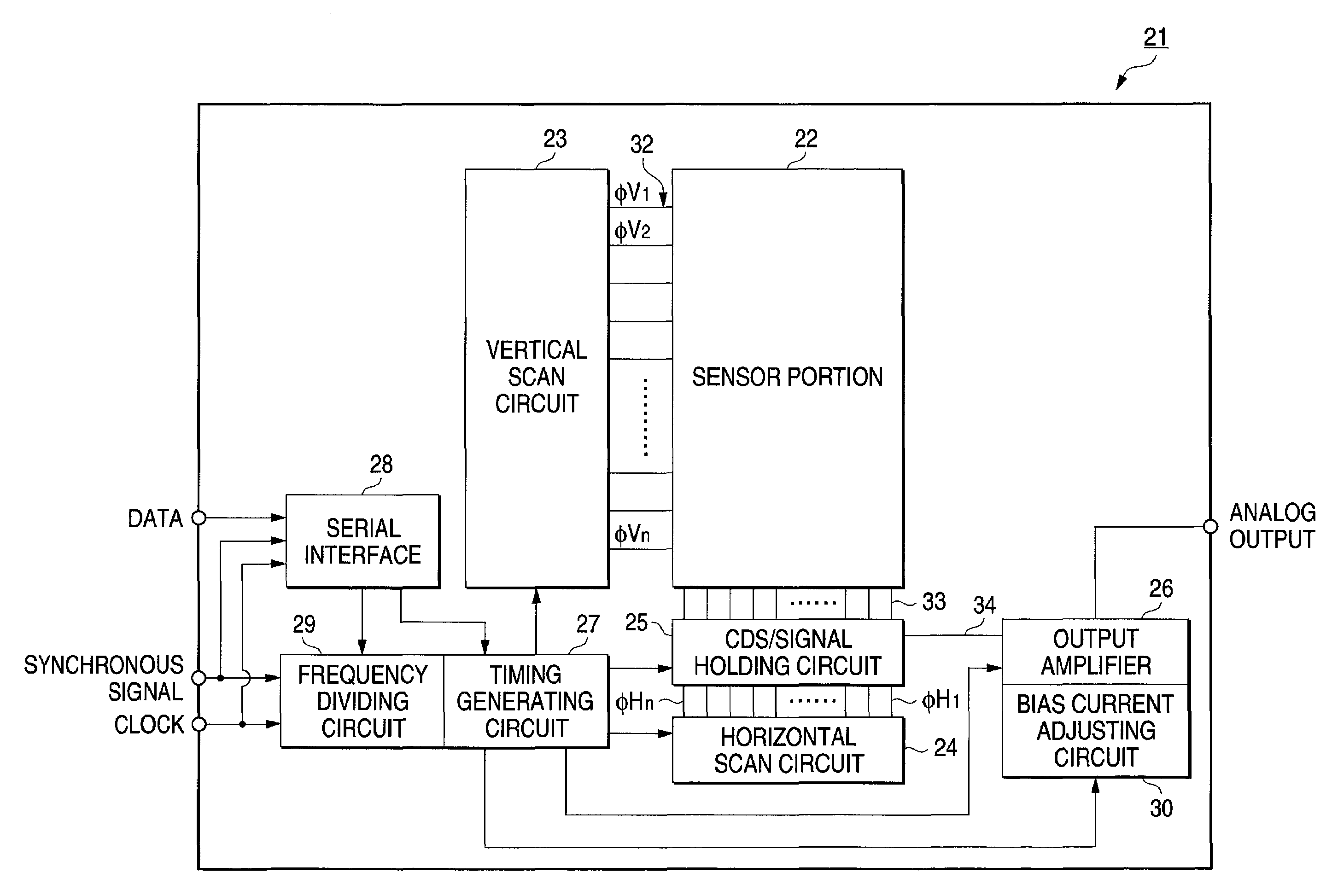
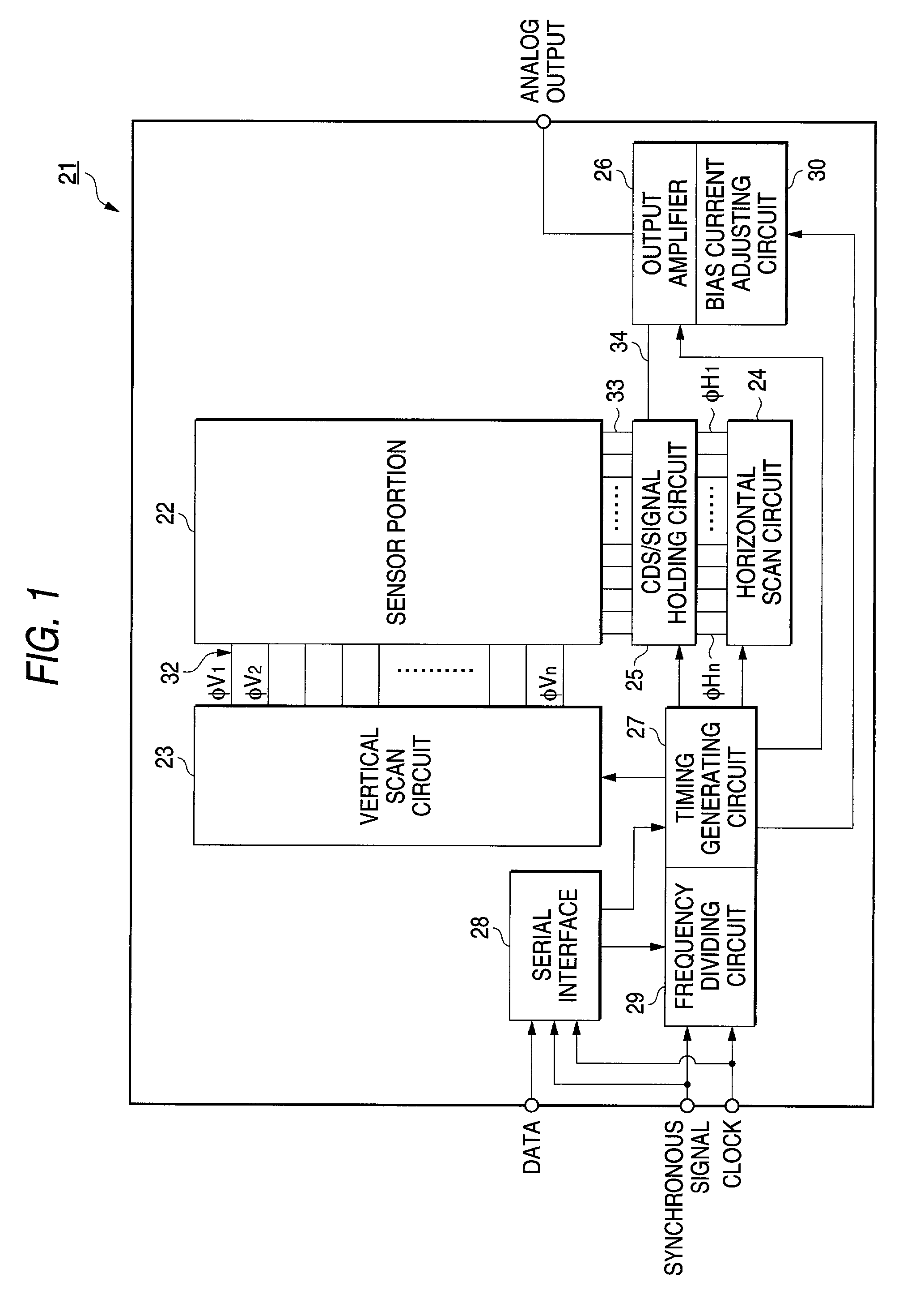
[0031]FIG. 1 shows a solid-state image pickup device of the present invention, that is, shows the construction of an MOS type solid-state image pickup device according to the present invention.

[0032]An MOS type solid-state image pickup device 21 includes a sensor portion 22 having many unit pixels arranged in a matrix form, each unit pixel comprising a photodiode for performing photoelectric conversion and an MOS switch element, a vertical scan circuit 23 and a horizontal scan circuit 24 for driving the sensor portion 22, a CDS / signal holding circuit 25 for receiving signals of pixels of one line of the sensor potion 22, an output amplifier 26, a timing generating circuit 27 for generating pulses for driving the respective parts, and a serial interface 28, and also includes a frequency dividing circuit 29 for frequency-dividing a clock signal in accordance with an instruction from the serial interface 28, and means for adjusting the f-characteristic of the output amplifier 26 (in th...

second embodiment

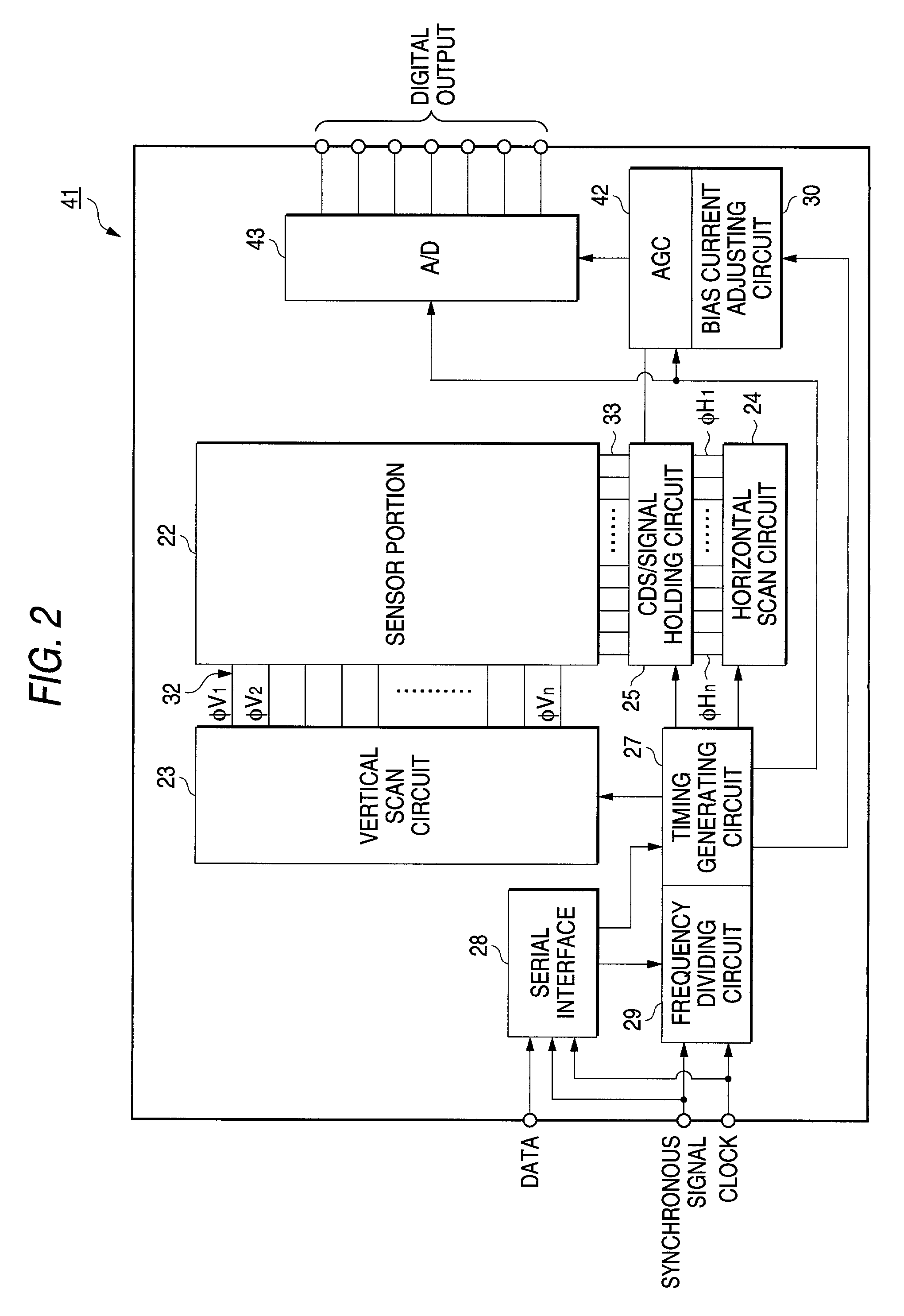
[0070]FIG. 2 shows the overall construction of the MOS type solid-state image pickup device according to the present invention.

[0071]In a solid-state image pickup device 41 according to this embodiment, the difference from the solid-state image pickup device 21 of the first embodiment of FIG. 1 resides in that an AGC (Auto Gain Control) circuit and an analog / digital (A / D) converter 43 are mounted to achieve a digital output. An AGC circuit 42 detects the signal level output from a CDS / signal holding circuit 25, amplifies the signal level at the proper gain corresponding to the signal level and then inputs the signal thus amplified to an A / D converter 43. The other construction is the same as shown in FIG. 1.

[0072]In this construction, since the power consumption in the AGC circuit 42 is increased, a bias current adjusting circuit 30 is equipped to the AGC circuit 42 to adjust the f-characteristic of the AGC circuit 42. The adjusting method is the same as described above. It is needl...


PUM


Abstract

A solid-state image pickup device including a sensor portion 22 having plural pixels arranged, a vertical scan portion 23 and a horizontal scan portion 24 for scanning the pixels of the sensor portion 22, an output portion 26 to which signals output from the sensor portion 22 are supplied, a bias current adjusting portion 30 for making the bias current of the output portion 26 variable, a driving signal generator 27 for supplying driving signals to the vertical scan portion 23, the horizontal scan portion 24 and said output portion 26, and an input portion 28 for supplying plural driving mode signals to the driving signal generator 27, wherein the driving frequency is made variable by the plural driving mode signals, and the bias current adjusting portion 30 is supplied with a signal for making the bias current variable in accordance with the plural driving mode signals.

Description

RELATED APPLICATION DATA[0001]The present application claims priority to Japanese Application(s) No(s). P2001-001685 filed Jan. 9, 2001, which application(s) is / are incorporated herein by reference to the extent permitted by law.BACKGROUND OF THE INVENTION[0002]1. Field of the Invention[0003]The present invention relates to a solid-state image pickup device applied to an image input system or the like, and particularly to an MOS type solid-state image pickup device. Further, the present invention relates to an image input device having an MOS type solid-state image pickup device mounted therein.[0004]2. Description of the Related Art[0005]Recently, a digital camera, a PC camera, an optical mouse, a portable TV telephone, etc. have been developed as an image input system using a solid-state image pickup device. These devices have been required to be low in driving voltage and power consumption not only from the image quality, but also from the viewpoint of battery using time and comp...

Claims


Application Information

Patent Timeline
Patent Type & Authority Patents(United States)
IPC IPC(8): H04N5/225H01L27/146H04N5/335H04N5/341H04N5/355H04N5/361H04N5/369H04N5/374H04N5/378
CPCH01L27/14621H04N5/3454H04N5/3456H04N5/3458H04N5/357H04N25/443H04N25/445H04N25/60H04N25/447H04N25/42
Inventor MABUCHI, KEIJIUENO, TAKAHISA
Owner SONY CORP
Why Eureka
Try Eureka